Here, a CAN bus controller is designed by using VerilogHDL. Firstly, the whole CAN bus controller is divided into three modules: interface logic management, register logic and CAN core module according to the protocol. Then, each functional module is designed with Verilog HDL hardware description language. The function of each module is simulated by using Modelsim software. Finally, the CAN bus controller of the design is verified by FPGA chip, and a 4-node CAN bus network including the FPGA CAN bus controller is connected. The test results show that the designed CAN bus controller can complete the set function.
CAN (Controller Area Network) is a serial communication bus defined by ISO. It is a new-generation network communication protocol that can effectively support distributed real-time control with high security level. It belongs to the field bus field. CAN was originally designed as a communication for microcontrollers in the automotive environment. It exchanges information between the electronic control devices on the vehicle and the ECU to form an automotive electronic control network. The current application fields have been extensive.
In recent years, chips supporting the CAN protocol have been continuously introduced, bringing great convenience to CAN bus users. With the increasing demand for fieldbus technology in China, CAN bus has become one of the most commonly used fieldbuses in China.
The development of the ECU electronic control unit based on the CAN bus is also the most popular research. Nowadays, the research on CAN bus chip is no longer limited to the research of single chip, but all the functional chips are concentrated on one chip to realize the function of a complete ECU.
The purpose of this project is to realize a bus controller supporting CAN2.0 protocol by using FPGA, and complete a general CAN bus controller soft IP core that can meet the CAN2.0 protocol, so that it can be easily integrated into other applications in future applications. Go in the system. In this paper, a CAN bus controller supporting CAN2.0 protocol is designed using VerilogHDL language, and the FPGA chip is tested in the CAN bus network to achieve the design goal. The innovation points are the register module in the CAN_Registers design, the transceiver part function of the bit stream processor, the test program, and the node circuit of the CAN bus controller based on the FPGA.
1 CAN bus controller design
1.1 CAN controller design flow
1.1.1 Functional design
Firstly, the CAN2.0 protocol was analyzed in depth, and the contents of the CAN bus protocol were mastered. Then, the functions of several typical CAN bus controllers were referenced and analyzed. Finally, the CAN bus controller SJA1000 produced by PHILPS was selected. Further analysis, mastered the functions of its various modules. On these basis, the functions of the designed CAN bus controller are planned as needed.
1.1.2 Design Description and Functional Verification
After the function design is completed, according to the function and referring to the CAN bus 2.0 protocol, the controller is divided into several functional modules, and the functions of each functional module are clarified. After determining the module and its functions, the design of each module was implemented in Verilog HDL language. Next, the entire design was functionally verified using Modelsim.
1.1.3 Logic synthesis
After the functional simulation, the CAN bus controller designed by the QUARTusII is logically integrated and configured into the FPGA.
1.1.4 Hardware Verification
After being configured into the FPGA, the designed FPGA-based CAN bus controller is used as a node to communicate with the node circuit using SJA1000 as the controller, and the function of the designed CAN bus controller is verified.
1.2 The overall design of the CAN bus controller
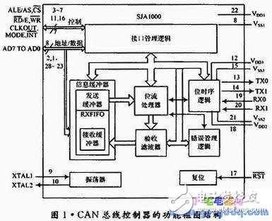
1.2.1 Functional structure of the controller SJA1000
The SJA1000 is a stand-alone CAN bus controller introduced by PHILIPS in 1997 for controller area networks in automotive and general environments. The SJA1000 is mainly composed of the following parts: interface management logic, transmit buffer, receive buffer, receive filter, bit stream processor, bit timing logic, error management logic. SJA1000 is a dual in-line integrated circuit, the functional block diagram shown in Figure 1.
1.2.2 Functional structure of the controller in this paper
The CAN controller designed in this paper refers to the structure of the SJA1000 controller. The functional basic framework contains three functional modules as shown in Figure 2.
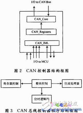
CAN_IML is the CAN bus controller interface logic. The main function is to interpret commands from the microprocessor, control the addressing of the CAN registers, and provide interrupt information and status information to the microprocessor.
CAN_Core is the core part of the CAN protocol controller. It completes all the functions of the data link layer in the CAN protocol and some functions of the physical layer, including the receiving filter of the LLC sublayer, overload notification and recovery management, and data encapsulation of the MAC sublayer. Disassembly, frame coding, media access management, error detection, error calibration, acknowledgment and serialization/deserialization, and bit coding/decoding, bit timing and synchronization of the physical layer. CAN_Registers is a register bank that external microprocessors can access directly through addresses. According to the functional block diagram, the program structure of the CAN bus controller is designed, as shown in Figure 3.
1.3 Design of each functional module of CAN bus
1.3.1 CAN_IML design
Refer to SJA1000 to design the interface of the FPGA CAN bus controller, as shown in Figure 4.
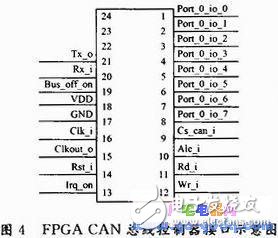
In the figure, Port_0_io_7 to Port_0_io_0 are address/data composite buses. Cs_can_i is the chip select input signal. Access to the CAN bus controller is allowed when Cs_can_i is zero. When Ale_i is 1, the register is allowed to be assigned. Rd_i and Wr_i are the read enable signal and the write enable signal of the microprocessor. IRQ_on is the interrupt output signal used to interrupt the microprocessor. Rst_i is the reset input and is used to reset the CAN interface. Clkout_o is the clock output signal provided to the microprocessor by the FPGA CAN controller. The clock divider register can disable the output of this pin. Bus_off_on controls the bus off and bus open interfaces, and Tx_o and Rx_i are connected to the transceiver to send and receive data to the bus.
1.3.2 CAN_Registers Design
The register module of the designed CAN bus controller includes the following registers: mode register, command register, status register, interrupt register, interrupt enable register, bus timing register 0~1, arbitration lost capture register, error code capture register, error alarm limit Register, Receive Error Counter, Transmit Error Counter, Acceptance Code Register 0 to 3, Acceptance Mask Register 0 to 3, Receive Information Counter, and Receive/Transmit Buffer.
1.3.3 CAN_Core Design
CAN_Core is the core of the entire CAN controller and is responsible for handling CAN protocols. The core module consists of four parts, and the structure is shown in Figure 5.
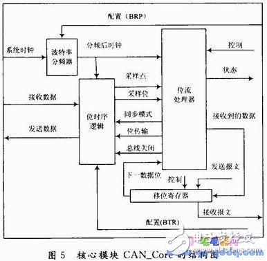
The following briefly introduces the bit stream processor and bit timing logic in the CAN_Core module.
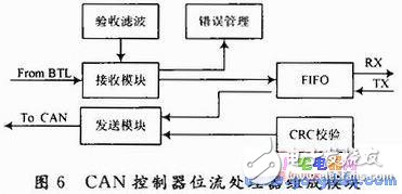
The bit stream processor is the generator that controls the flow of data in the CAN bus controller. It also performs functions such as error detection, arbitration, padding, and error handling on the bus. There are mainly six modules, such as receiving module, transmitting module, error management module, CRC check, acceptance filter, FIFO, etc., as shown in Figure 6. Among them, the CRC check, FIFO, and acceptance filter have been designed by others in the executed project.
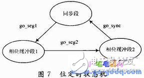
The design of the bit timing logic includes bit timing design, sampling point design, and bit synchronization design. The following is an example of positioning when introducing positioning.
Bit Timing Design A state machine with three states is used in the bit timing design. The three states correspond to the sync segment and the phase buffer segment 1 and the phase buffer segment 2, respectively. The short time occupied by the propagation segment has no special meaning in control, only as the propagation delay of the physical layer, so it is not designed into the state machine. The state machine design of the bit timing part is shown in Fig. 7.
Then using ModelSim software to simulate the function of each module and the whole CAN bus controller, the simulation results show that the design goal is achieved.
Biogas Generator,Biogas Power Generator,Biogas Electric Generator,Biogas Energy Generator
Jiangsu Vantek Power Machinery Co., Ltd , https://www.vantekpower.com