With the rapid development of mobile communication technology, the requirements for high speed and low power consumption of radio frequency circuits are increasing. The frequency synthesizer based on the phase-locked loop (PLL) structure is an important part of the front-end circuit of the transceiver, and plays an important role in providing a pure local oscillator signal for the mixer. In the PLL, the voltage-controlled oscillator (VCO) and the prescaler (Prescaler) are the two modules operating at the highest frequency, which are the main bottlenecks that limit the operating frequency of the PLL, thus increasing the operating speed of the prescaler. It is a key factor in solving the upper limit of the PLL operating frequency. In order to meet the requirements of high-frequency communication, high-speed, low-power optimization design of the prescaler and VCO must be performed.
The dual-mode prescaler uses a D flip-flop as the main unit. In recent years, many high-speed D flip-flops with different structures have emerged. The first is a static SCL structure that evolved from the ECL circuit structure. Compared with the traditional static crossover, it works faster because of its small swing. However, the 2-way circuit of the typical SCL structure requires at least 18 MOS transistors including the tail current source. The MOS transistor cannot be small in size, resulting in a large input capacitance or even exceeding the capacitance of the tube itself, so the power consumption of the SCL divider Higher. The second type is a dynamic TSPC (single-phase clock) structure, which uses a single-phase clock TSPC technology to reduce the number of components constituting the frequency divider, which can increase the operating speed of the circuit, and the power consumption of such a circuit is extremely low. Often used in pre-frequency dividers. The shortcoming of the TSPC divider is poor noise performance because the dynamic single-ended structure is more susceptible to noise than the SCL structure. The third type is an inducted-locked circuit. Due to the use of an inductor, it is too bulky and difficult to apply, and is rarely used. Which circuit structure should be used depends on the situation.
In this paper, a dynamic TSPC structure is used to design a dual-mode prescaler suitable for WLAN IEEE802.11a standard using TSMC 90nm 1P9M 1.2VCMOS technology, featuring high speed, low voltage and low power consumption.
1 circuit design1.1 Overall circuit architecture
The basic structure of the dual-mode prescaler is shown in Figure 1. It consists of three parts: a synchronous 2/3 divider, a divider chain consisting of an asynchronous divide-by-2 divider, and a feedback section. The control signal MC controls the frequency division ratio, which is 32 divided when MC=1, and 33 divided when MC=O.
Figure l Dual-mode pre-frequency divider structure
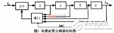
The design is based on the above conventional structure, and the purpose of reducing power consumption is achieved by reducing the number of MOS tubes in the high frequency synchronous frequency divider unit.
1.2 Synchronous Divider Design
The block diagram of the synchronous 2/3 divider is shown in Figure 2. It is the most active part of the entire divider and is a key part of determining the speed and power consumption of the prescaler.
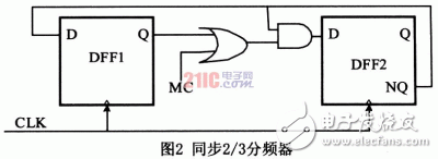
When MC is logic high, the circuit achieves a divide by 2; when MC is at a logic low level, the circuit achieves a divide by three. The use of a synchronous 2/3 frequency divider greatly reduces the number of MOS transistors operating in the high frequency portion, so that the power consumption of the synchronous portion is reduced. At the same time, the AND gate is designed in the D flip-flop. This integrated AND gate flip-flop not only simplifies the circuit design, but also avoids the influence of parasitic parameters caused by the separate design of the logic gate, reducing the speed loss, thus greatly reducing the work speed and power consumption. Contradictions.
1.3 Optimizing power consumption
From the above analysis, it can be seen that the maximum power consumption of the circuit comes from the synchronous 2/3 frequency divider, but whether it is a synchronous 2/3 frequency divider or an asynchronous frequency divider chain, D flip-flops must be used, so the design is high speed and low. The D flip-flop for power consumption is the key to affecting the speed and power consumption of the entire divider.
Figure 3 shows a commonly used Yuan-Svensson type D flip-flop (falling edge trigger). This circuit uses dynamic CMOS technology and consists of an N-C2MOS stage, a P-PrechargeCMOS stage and a P-C2MOS stage from left to right. Compared with the traditional static frequency divider, its performance has been significantly improved, but since most MOS tubes are both the pre-stage load tube and the rear-stage drive tube, each level of three MOS tube overlays There is a big RC delay, so even if you reduce the size, you can't increase the speed. To this end, we have improved the C2MOS circuit in Figure 3, replacing the N-C2MOS with a clocked pseudo PMOS inverter, so that the number of MOS transistors and the load capacitance are reduced. Similarly, the clocked pseudo NMOS inverter is used instead of PC2MOS to form the dynamic ratio latch shown in Figure 4. When the clock signal is low (high) level, the latch operates in the evaluation (hold) mode, and Yuan- The D-flip-flop of the Svensson structure has a lower RC, thus reducing power consumption and transmission delay.
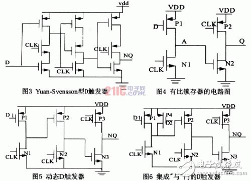
It should be noted that when the latch of FIG. 4 operates in the evaluation mode (CLK is low), if the input signal D changes from a high level to a low level at this time, the state of the output Q is inverted. Causes misoperation. Therefore, it is necessary to add a primary clock pseudo PMOS at the input end of the latch, as shown in FIG. 5, to prevent the voltage of the input terminal D from being flipped from high to low when the latch shown in FIG. 4 operates in the evaluation mode. The output of the latch can only be changed once in a single cycle. Figure 5 is the negative edge-triggered dynamic D flip-flop used in this paper. Compared with the YuanSvensson D flip-flop shown in Figure 3, the number of transistors of the dynamic D flip-flop is reduced by three, which enhances the driving ability of the clock and improves not only The operating frequency of the circuit is greatly reduced. At the same time, the AND gate is integrated into the DFF, as shown in Figure 6. The simulation results show that the D-flip-flop of this integrated AND gate has a certain increase in the working speed, and also reduces the power consumption of the circuit. In the synchronous 2/3 divider, DFF1 uses a D flip-flop without an AND gate, and DFF2 uses a flip-flop with an AND gate.
1.4 asynchronous divide by 2 divider
Indoor Fixed LED Display is a popular product for its high quality, every year sold to at least 80,000 pieces around the world, including Europe, North America, southeast Asia.Compared to other indoor LED display in the market, its biggest advantage is that it can display high-definition images while maintaining low power consumption.Besides, it adopts Die casting aluminum cabinet which is ultra-thin and ultra-light and owns good heat dissipation.Easy to install and maintain and suitable for multiple indoor scenes.
Application:
* Business Organizations:
Supermarket, large-scale shopping malls, star-rated hotels, travel agencies
* Financial Organizations:
Banks, insurance companies, post offices, hospital, schools
* Public Places:
Subway, airports, stations, parks, exhibition halls, stadiums, museums, commercial buildings, meeting rooms
* Entertainments:
Movie theaters, clubs, stages.
Indoor Fixed LED Display,Led Wall Display,Video Wall Display,Outdoor Led Screen Display
Guangzhou Chengwen Photoelectric Technology co.,ltd , http://www.cwstagelight.com