There are two main types of flash memory chips on the market, namely NAND Flash (Not And Flash ROM) and NOR Flash (Not Or Flash ROM). The former has the characteristics of large capacity, fast reading and writing speed, small chip area, high cell density, fast erasing speed and low cost, and is more suitable for embedded systems of large-volume data storage. Windows is still the mainstream of desktop systems today, providing natural support for the FAT file system. However, as far as technology is concerned, the FAT file system is not suitable for Flash, because the Flash device is not a block device [1]. In order not to damage the compatibility and apply the FAT file system in the NAND flash memory, the FTL file layer of the flash translation layer is proposed internationally. (Flash TranslaTIon Layer) solution.
1 NAND Flash embedded storage system structureThe design of NAND Flash-based storage systems must first solve the bad block problem. Since NAND Flash itself has inherent bad blocks and randomly generates bad blocks in erasing and programming, in order to improve the reliability of the device, these two operations should be dispersed in different blocks of flash memory to avoid excessive operation on a block. .
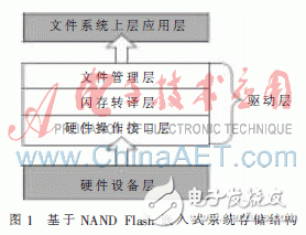
The general NAND Flash embedded storage system driver structure is divided into three levels: the bottom layer is the hardware operation interface, which is responsible for connecting the main control chip to the control pin of the Flash. The firmware in this aspect mainly implements the physical operation of the NAND Flash; The middle layer is the Flash Translation Layer NFTL (NAND FTL), which is a software module packaged in the Flash driver. Its function is to simulate Flash into a block device similar to a disk, so that NAND Flash is like ordinary to the upper operating system. The disk is accessed as well. This layer mainly encapsulates some special complex management control functions; the top layer is the file management layer, which functions like a general file system on a common disk, and provides a standard file operation interface to the upper layer. The schematic diagram of the storage structure of the embedded system based on NAND Flash is shown in Figure 1.
According to the above two aspects, it is necessary to implement bad block management in the driver and block simulation. Therefore, there are two methods available [2]: one is to solve the bad block problem in the upper file system, and the driver layer only implements itself. The function of the file system provides a constant interface to the driver layer, providing reliable and transparent services for upper-layer applications. This method is simpler, the development cycle is shorter, but it is only very adaptable to the embedded system of a specific application; the second method is to solve the bad block problem in the NFTL of the driver layer, and the unreliable NAND Flash virtual As a reliable storage device, providing reliable and transparent services for the upper file system, this method is more complicated than the first one, but this method has strong portability and can completely cut off the connection with the file system, and other file systems are also the same. Be applicable.
This paper is based on Samsung's NAND Flash K9F2808U0C as a memory chip, designed a method to achieve bad block management and continuous data reading on NFTL.
2 design ideas2.1 Flash space division
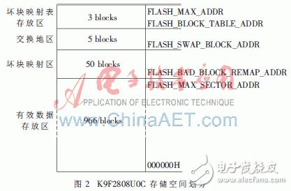
The K9F2808U0C is a 16 MB & TImes; 8 bit NAND Flash with a total of 1,024 Blocks, 1 Block = 16 KB, 32 Page/Block, 1 Page=528 B=(512 B+16 B), of which 16 B is the spare area, mainly Store NAND Flash factory bad block mark, ECC check code and user-defined area. The K9F2808U0C address space is 24 bits and is sent to the address latch of the NAND Flash in three cycles. The addresses used in this document are all byte addresses, and the data type is DWORD(4 B).
The storage space of the K9F2808U0C is divided into four areas: a bad block mapping table storage area, a swap block area, a bad block mapping area, and an actual data storage area. The space managed by the file system is the actual data storage space, as shown in Figure 2.
2.2 Each partition macro definition
#define FLASH_BLOCK_SIZE 0x40000 //16 KB/Block
#define FLASH_PAGE_SIZE 0x200 //512 B/Page
#define FLASH_SECTOR_SIZE 0x200
//1Page=1Sector(only K9F2808U0C)
#define FLASH_BLOCKS_TABLE 3//Block block mapping table storage block number
#define FLASH_SWAP_BLOCKS 5 //Number of blocks in the swap area
#define FLASH_BAD_BLOCKS_REMAP 50
/ / The number of blocks in the bad cluster remap area
#define FLASH_MAX_ADDR 0xFFFFFF
/ / Flash maximum byte address
The formula for calculating the first address of each partition:
FLASH_BLOCK_TABLE_ADDR=FLASH_MAX_ADDR+
1-3*FLASH_BLOCK_SIZE);
FLASH_SWAP_BLOCK_ADDR=(FLASH_BLOCK_
TABLE_ADDR-5*FLASH_BLOCK_SIZE);
FLASH_BAD_BLOCK_REMAP_ADDR=(FLASH_SWAP_
BLOCK_ADDR-50*FLASH_BLOCK_SIZE);
FLASH_MAX_SECTOR_ADDR=(FLASH_MAX_ADDR-
3*FLASH_BLOCK_TABLE_ADDR-5*FLASH_SWAP_
BLOCK_ADDR-50*FLASH_BAD_BLOCK_REMAP_ADDR);
The maximum byte address managed by the file system.
Any address Addr:
Block address: Addr&(~(FLASH_BLOCK_SIZE-1));
Intra-block offset address: Addr&(FLASH_BLOCK_SIZE-1);
Page in the block: (Addr&(FLASH_BLOCK_SIZE-1))/FLASH_
PAGE_SIZE;
2.3 partition function design
The bad block mapping area stores 3 pieces of bad block information BBI (Bad Block InformaTIon) table. Replicating 3 copies is to prevent the system from suddenly powering down, causing data loss in the BBI table. The last three blocks were chosen, mainly for firmware design. When the Flash is powered on for the first time, the firmware program reads the Flash ID, obtains the capacity of the device, and then looks for the BBI table from the last piece of Flash. If the last block does not find the BBI table, the block is considered to be a bad block. The search is searched, and so on, until it is found in the reserved 3 blocks, and its data is read into the RAM opened by the master chip. If it is not found, the firmware thinks that the slice of Flash does not have a BBI table.
The swap block area is used to temporarily store data when erasing or writing to the NAND Flash, and a total of 5 blocks are allocated. Five blocks were chosen for reliability design. Record the swap block status with an array FlashSwapBlockStatus[FLASH_SWAP_BLOCKS]: valid or corrupt. At initialization, the firmware considers all swap blocks to be valid blocks. When subsequently erasing or writing, the flash status register is read to determine the true state of the swap block and recorded in the array. The management of the switch block returns the currently available switch block address or the switch block address currently being used around the firmware request and determines that the switch block state currently used by the tag is bad.
The bad block mapping area is when the host writes data to the data area, when the current block (data area) is detected as a bad block, the data is written into the corresponding good block in the bad block mapping area, and the blocks of the two blocks are The address is recorded in the BBI table. If the host wants to access the current block (data area), it only needs to read the BBI table to find the corresponding mapping block, thus replacing the access of the bad block. This makes the logical block address LBA (Logical Block Address) seen by the file system become contiguous, but in fact the physical block address PBA (Physical Block Address) may not be continuous. The above method is the essence of bad block management. For the conservative design, a total of 50 blocks were selected as remap blocks. Use the array FlashRemapBlockStatus[FLASH_BAD_BLOCKS_REMAP] to identify the status of the bad block map area: unused, used, or corrupted. At initialization, all blocks in the bad block mapping area are considered to be good blocks.
3 NFTL bad block management design3.1 Building a BBI Table
Store the BBI table with an array of FlashBadBlockTable[2][FLASH_BAD_BLOCKS_REMAP]. The first dimension is the block address of the bad block (data area), and the second dimension is the mapping block address (re-blocking block).
The BBI table can be constructed by reading the bad block flag set by the manufacturer in the Flash spare area to identify the bad block when the Flash is first powered on, and establishing a bad block mapping table. The initialization time is proportional to the capacity of the Flash; or by reading All block contents of NAND Flash are compared with 0xFF [3]. If they are not the same, they represent bad blocks. This method is only for the new flash memory, and the BBI table is built for a long time, and the occupancy of the main control chip is high. Another method is to not create a bad block table when the Flash is first powered up, and think that all the current blocks are good. Block, find bad blocks in subsequent operations, and update the BBI table. This article chooses the latter method.
3.2 Design of bad block mapping table area
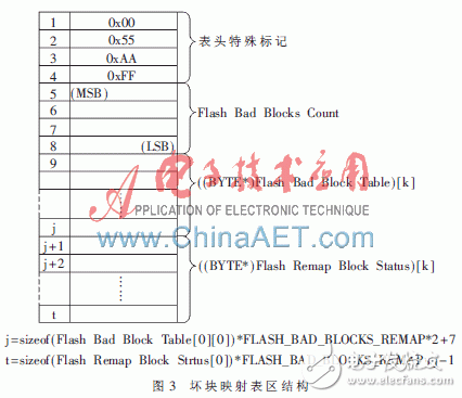
The BBI table is saved in a special way, and the BBI table is later identified by the reverse of this way. The design method of the three blocks of the bad block mapping table area is as follows:
(1) A special flag is placed at the first byte of the last page of each block to identify whether the block is ready to be erased: 0xFF indicates that it is not ready to be erased; 0x00 indicates that the block is ready to be erased [4] .
(2) Write 0x00 at the first byte of the second-to-last page of each block, indicating that the block stores BBI table data; and store the checksum in big-end mode at the 2nd, 3rd, 4th, and 5th bytes, To verify the correctness of all data stored in the block. The remaining bytes of this page are written as 0xFF.
(3) Write on the first page: the header special mark (0x0055AAFF), the bad block total (FlashBadBlockCount), the BBI table (FlashBadBlockTable), and the remap block state (FlashRemapBlockStatus). The structure is shown in Figure 3.
500W Digital Tv Transmitter,Wireless Digital Tv Transmitter,Digital Tv Broadband Transmitter,Digital Tv Signal Transmitter
Anshan Yuexing Technology Electronics Co., LTD , https://www.yxhtfmtv.com