>>> 4.4.1 Interrupt and event driven
The clock signal and the data/control line are used regardless of which bus is used, and the clock signal is controlled by the MCU master. The SPI in the signal line for control is 4, in addition to the transmitted signal, there is a chip select signal, and the host specifies which device is the target object by the validity of the signal.
> > > 4.6.1 Introduction to SPI Bus
Here, take the LPC824 as an example to introduce the principle and application design of the host SPI.
SSEL: Chip Select Input
When the SPI is used as the master, the SSEL signal is driven to the active state before the serial data is started, and the signal is released after the serial data is transmitted, making it inactive. The default SSEL is active low and can also be selected as active high. When the SPI is a slave, any SSEL signal that is active indicates that the slave is being addressed.
MOSI: master output slave input
The MOSI signal transfers serial data from the host to the slave. When the SPI is the master, the serial data is output from the MOSI; when the SPI is the slave, the serial data is input from the MOSI.
MISO: master input slave output
The MISO signal transfers serial data from the slave to the host. When the SPI is the master, the serial data is input from the MISO; when the SPI is the slave, the serial data is output to the MISO.
SCK: clock signal
SCK Synchronous data transfer clock signal. It is received by the master-driven slave. When the SPI interface is used, the clock can be programmed to be active high or active low.
> > > 4.6.2 74HC595 interface
Under the same clock signal, the 74HC595 implements serial input/parallel output conversion of data. In addition to the 8 parallel outputs, the 74HC595 has 5 input controls, of which 

 Q 7 ~ Q 0 output; at the same time
  V CC to ensure that the 74HC595 is permanently strobed. There are also three input terminals: CP clock signal terminal, D data input terminal and STR latch signal, which are respectively connected to SCK, MOSI and SSEL of MCU, as shown in Figure 4.18.
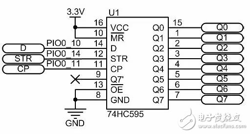
Figure 4.18 74HC595 circuit diagram
Under the action of the rising edge of the CP clock signal, it is guaranteed that the binary data loaded on the D side is sequentially sent to the 74HC595. When the data shift is completed, under the action of the rising edge of STR, the data will be outputted once at Q 7 ~ Q 0 , thus ensuring that the data at the output remains unchanged during the shifting process.
The MiniPort-595 module uses the 74HC595 to expand 8-channel I/O, which can directly drive the LED display module. The definition of the M4 function corresponding to the AMPort-Core MiniPort interface is shown in Figure 4.19(b). The function definition of the MiniPort-595 module output signal pin J2 is shown in Figure 4.19(c).
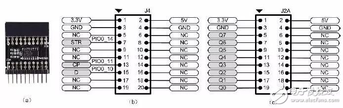
Figure 4.19 595 Module Physical and Control Interface Definition
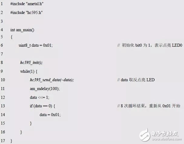
Suppose you want to serially transfer 1000 0000 to the parallel output terminals Q 7 ~ Q 0 of the 74HC595. This data is sent to the serial data input terminal D bit by bit from Q 7 ~ Q 0 under the action of the clock pulse. After 8 clock pulses have elapsed, 10000000 is output in parallel at Q 7 ~ Q 0 . AMetal provides the corresponding hc595.h interface for the 74HC595, as detailed in Listing 4.44.
Listing 4.44 hc595.h interface
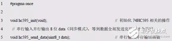
It can be seen that by calling hc595_send_data() after initializing the 74HC595 related operation, the serial input outputs an 8-bit binary number in parallel, and the output pin of the 74HC595 is used as an 8-bit I/O port. Previously, 8 LEDs were controlled to use 8 I/O ports. Now with the 74HC595, more I/O ports can be saved for other uses.
Obviously, as long as the AMPort-Core host, the MiniPort A of the MiniPort-595 module and the MiniPort B of the MiniPort-LED module are directly inserted, the schematic diagram is shown in Figure 4.20. See Figure 4.21(a). After the combination, the MPort's MiniPort interface J4 port function definition is shown in Figure 4.21(b). The MCU controls the 74HC595 chip to drive 8 LEDs through the STR, CP and D ports. See Listing 4.45 for details. .
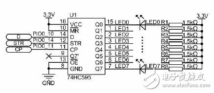
Figure 4.20 8-Output I/O Expansion
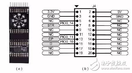
Figure 4.21 Module combination physical and control interface definition
Listing 4.45 74HC595 Universal Interface Sample Program
Obviously, the 74HC595 can also be used to drive the 8 segments of the digital tube. The schematic diagram is shown in Figure 4.22.
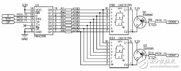
Figure 4.22 2-digit digital tube driver circuit
The MiniPort A (pin header) of the AM824-Core and MiniPort-595 modules and the MiniPort B (mother socket) of the MiniPort-View module can be directly inserted into each other. For details, see Figure 4.23(a). After the combination, the corresponding MCU is used. The definition of the MiniPort interface J4 function is shown in Figure 4.23 (b). In addition to using the STR, CP, and D ports to control the 74HC595, the MCU also needs to use COM0 and COM1 to control the position of the digital tube.
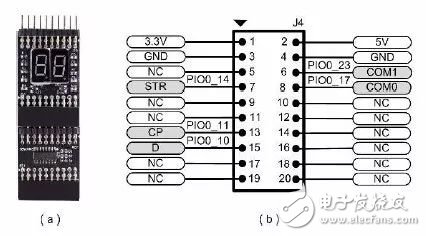
Figure 4.23 Module Combination Physical and Control Interface Definition
In fact, the 74HC595 is used directly with I/O to drive the digital tube. The only difference is that the segment code output method is different. Therefore, you only need to modify the segment code transfer function and add the implementation code to digitron1.c. See Listing 4.46 for details. .
Listing 4.46 adds the relevant function of the 74HC595 driver
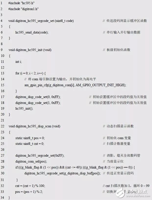
Since the user does not directly call digitron_hc595_segcode_set(), only digitron_hc595_init() and digitron_hc595_disp_scan() are added to the digitron1.h interface shown in Listing 4.47.
Listing 4.47 digitron1.h
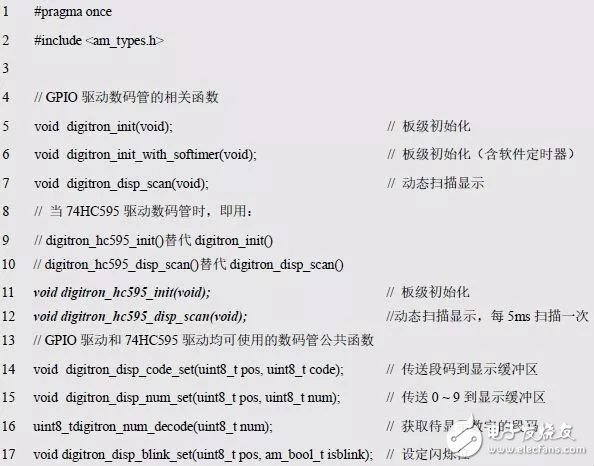
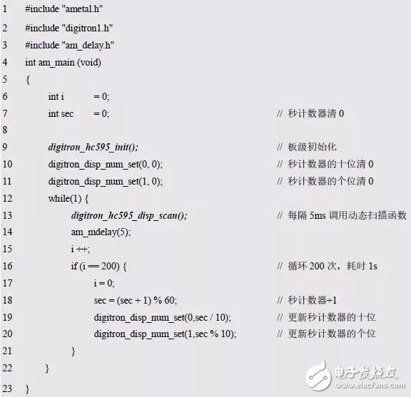
When using the 74HC595 to drive the digital tube, just call the relevant function, as shown in Listing 4.48.
Listing 4.48 74HC595 driver digital tube implementation seconds counter sample program
4.7 I 2 C bus
> > > 4.7.1 Introduction to I 2 C Bus
The I 2 C bus (Inter Integrated Circuit) is a two-wire bus developed by NXP to connect microcontrollers and peripheral devices. It not only has very simple hardware circuits, but also has great reusability and portability. The I 2 C bus is not only suitable for communication between devices in the board, but also enables long-distance signal transmission between the board and the board through the repeater, so it is very easy to build system-level electronic products using I 2 C devices. Development Platform. Its characteristics are as follows:
The bus only needs 2 signal lines, which reduces the space of the board and the number of chip pins, reducing the interconnection cost;
Multiple devices can be mounted on the same I 2 C bus, and the devices are distinguished by different addressing, so no additional I/O or address decoder is needed;
Very easy to implement the self-test function of the I 2 C bus, in order to find out the abnormal situation of the bus in time;
The bus is electrically compatible. The I 2 C bus stipulates that the devices are interconnected with open-drain I/O. Therefore, 3V/5V logic level compatibility can be easily achieved by selecting appropriate pull-up resistors.
Support multiple communication methods, one master is the most common communication method. It also supports dual-host communication, multi-master communication and broadcast mode;
The communication rate is high, its standard transmission rate is 100Kbps (100K bits per second), and 400Kbps in fast mode. According to the later revised version, the bit rate can be as high as 3.4Mbps.
> > > 4.7.2 LM75B Interface
The AM824-Core selects the LM75B digital temperature sensor that is compatible with the LM75A and consumes only 1μA in shutdown mode.
1. characteristic
The LM75B is a digital temperature sensor chip with I 2 C interface from NXP Semiconductors. Its key features are as follows:
The device address is 1001xxx, and 8 devices can be expanded on the same bus;
Power supply range: 2.8 ~ 5.5V, temperature range: -55 ~ 125 ° C;
The 11-bit ADC provides a temperature resolution of 0.125 ° C;
Accuracy: ± 2 ° C (-25 ~ 100 ° C), ± 3 ° C (-55 ~ 125 ° C).
The pin arrangement of the LM75B is shown in Figure 4.24. The slave address is 0x90, A0~A2 are address selection bits 0~2, and the pull-up resistor must be added to the SCL serial clock input and SDA serial data signal line. When the chip overheats, the output is turned off.
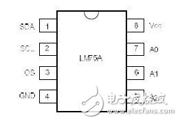
Figure 4.24 LM75B pin diagram
2. Application circuit
The LM75B typical application circuit is shown in Figure 4.25. R5 and R6 are pull-up resistors for the I 2 C bus. Since there is only one LM75B on the board, you can directly ground the A0~A2 pins of the chip without considering the address of the chip. The OS is the overheating output of the chip, and the external thermostat can be realized by an external relay device. Since the temperature is measured by the MCU, this pin can be left floating. As long as (J13_1, J13_2) and (J11_1, J11_2) are shorted, SDA and SCL are connected to PIO0_18 and PIO0_16, respectively.

Figure 4.25 LM75B Application Circuit Diagram
Figure 4.26 shows the heating circuit of the AM824-Core. The resistance of R32 is 20~50Ω (2W). Short-circuit J14_2 and J14_3 to connect the heating resistor R32 soldered near the LM75B to the KEY. When the KEY button is pressed, R32 starts to heat up. At this time, the heat generated by the resistor is transmitted to the bottom of the LM75B through the thicker wire. Then the LM75B will follow the heat. If the resistance is smaller, the larger the current passed, the more heat is generated. When the button is pressed, the circuit is turned on. At this time, the temperature rise circuit can be observed through the temperature measuring circuit.
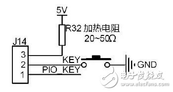
Figure 4.26 Heating circuit
3. Temperature measurement
For the LM75B, AMetal provides the corresponding software package, the function prototype is:

Obviously, using these two common interfaces, it is easy to read the current temperature value. Since there are only two digital tubes, only the integer part is displayed; when the temperature is negative, it does not display negative, only the temperature value is displayed. See Listing 4.49 for details.
Listing 4.49 LM75 Temperature Reading and Display Sample Program
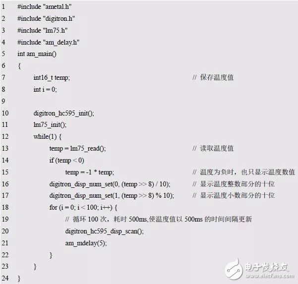
After the program is compiled and downloaded to the development board, if the digital tube displays 28, the current temperature is 28 °C. If the heating button is pressed, the low-resistance heating resistor R32 starts to heat up, and the displayed temperature value will continue to rise.
When the temperature value is displayed, the temperature value is shifted to the right by 8 bits. This is because the value read by lm75_read() is 256 times the actual temperature, so the actual temperature should be the value read by 256.0. At the same time, since there is no need to display the fractional part, shifting 8 bits directly to the right means dividing by 256, leaving only the integer part.
> > > 4.7.3 Thermostat
The following will be combined with the previously written program, using LED, buzzer, digital tube, matrix keyboard and temperature acquisition to achieve a simple thermostat.
1. Function introduction
The temperature is collected on the digital tube using the standard I 2 C interface LM75B temperature sensor. Since there are only two digital tubes, only the integer part is displayed; when the temperature is negative, the negative value is not displayed, only the temperature value is displayed.
The upper temperature limit and the lower temperature limit can be set. When the temperature is higher than the upper limit or lower than the lower limit, the buzzer will beep.
2. Status indication
During the adjustment process, two LEDs are used for status indication, and J9 and J10 can be connected with a short circuit jumper.
LED0 is on: it indicates that the current value is the upper limit value, and the digital tube displays the upper limit value;
LED1 is on: it indicates that the current value is the lower limit value, and the digital tube displays the lower limit value;
Two lights flashing: indicating normal operation, the digital tube displays the ambient temperature value.
3. Instructions
When setting the upper and lower limits, a total of 4 buttons are used. which is:
SET button: Used to enter the setting state. After clicking, first enter the temperature upper limit setting, click again to enter the temperature lower limit setting, and click again to return to the normal running state;
Left/Right Shift key: Used to switch the currently adjusted bit (one digit/ten digit). When entering the setting state, the currently adjusted bit will flash continuously; click this button to switch the currently adjusted bit, switch from one bit to ten digits, or from ten digits to one digit;
Add 1 key: When entering the setting state, the currently adjusted bit will continue to flash, press this key to increase the value on this bit by 1;
Subtract 1 key: When entering the setting state, the currently adjusted bit will flash continuously. Press this key to increase or decrease the value on this bit by 1.
(1) Set the upper limit
Press the SET button for the first time to enter the upper limit setting. At this time, LED0 lights up, the digital tube displays the upper limit temperature, and the single digit stops flashing. Press “Add 1†or “Subtract 1†to adjust the value of the current flashing position. Press “Left/Right†to switch the currently adjusted bit.
(2) Setting the lower limit value
On the basis of setting the upper limit value, click the SET button again to enter the lower limit setting. At this time, LED1 lights up, the digital tube displays the lower limit temperature, and the single digit blinks. Press “Add 1†or “Subtract 1†to adjust the value on the current flashing position. Press “Left/Right†to switch the currently adjusted bit.
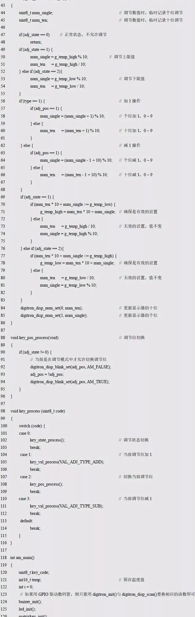
4. Function realization
As shown in the program list 4.50, the sample program of the thermostat is more complicated in the program. In order to make the program structure clearer, three functions are written for each of the three buttons: switching state (KEY0), switching the current adjustment bit (KEY2), and adjusting the current bit value (KEY1 and KEY3). Each function is directly in key_process(). Called in the button handler. The other parts are completed in the main(1) main loop, mainly completing three things: temperature value acquisition, once every 500ms; keyboard scanning, every 10ms; digital tube scanning, every 5ms.
Listing 4.50 Comprehensive Experimental Sample Program
Portable high efficient travel charger, can charge multi devices at the same time, every port output mini 5v 1a, max 5v 2.1a. We can meet your specific requirement of the products, like label design. The plug type is US/UK/AU/EU. The material of this product is PC+ABS. All condition of our product is 100% brand new.
Our products built with input/output overvoltage protection, input/output overcurrent protection, over temperature protection, over power protection and short circuit protection. You can send more details of this product, so that we can offer best service to you!
Usb Charger,Universal Travel Adapter,Intelligent Usb Charger,Travel Adapter
Shenzhen Waweis Technology Co., Ltd. , https://www.waweispowerasdapter.com