Abstract: This paper introduces the characteristics of LED fluorescent lamp driving, and designs a practical capacitive buck LED fluorescent lamp driving circuit, focusing on the selection principle of key component parameters. The PSp ice simulation software was used to verify the feasibility of the designed circuit. On this basis, the physical circuit was fabricated and used as the 12W T8 standard LED fluorescent lamp power supply. The experiment proves that the circuit is stable and reliable, low cost, and is suitable for a variety of low power LED drivers.
0 Preface
Since the first visible red LED was discovered using phosphide on a gallium arsenide substrate since the late 1960s, with the breakthrough of technologies such as semiconductors and LED packaging, the power levels of single-chip red, green, blue, and white LEDs And brightness is constantly improving. At present, high-power white LEDs have reached 70 lm / W. With the significant improvement in LED efficacy, lifetime and light color, it has huge market potential in the fields of display, backlight, decoration and lighting. Although the application level of LED is expanding, the life and light efficiency are higher than traditional lighting, but the cost is relatively high. The cost of LED light source is up to 50%~90% of the total cost. There is still room for improvement in lighting source technology, and high-power LED Heat and light efficiency issues are highlighted, which limits the further application of LEDs in the field of lighting.
At present, low-power LEDs will be connected in parallel and in series when used. As long as one LED is short-circuited or open-circuited during use, the small piece or the entire LED will be extinguished, which will affect the lighting effect. Therefore, the research is simple and inexpensive. Significance. According to the current application status of LED fluorescent lamps, a simple and reliable 12W standard T8 LED fluorescent lamp driving circuit is designed.
1 fluorescent lamp circuit design
1. 1 LED fluorescent lamp driver
At present, two types of drive circuits are widely used in low-power lighting products: constant current drive and regulated drive. The current output from the former circuit is constant, and the output voltage varies with the load. Constant current driving usually uses a constant current IC. When used, the maximum voltage value required by the IC is high, which limits the number of LEDs used. The latter output voltage is fixed and the output current varies with the number of loads (LEDs). Experiments have confirmed that due to the large discrete value of the forward voltage drop in the LED package, and the LED brightness output is proportional to its current, the LED brightness consistency is poor, but the string brightness can be averaged by adding a suitable resistor. Low-end lighting market.
1. 2 LED fluorescent lamp circuit design
The schematic diagram of the LED fluorescent lamp driving circuit is shown in Figure 1.
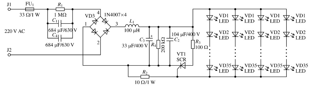
Figure 1 LED fluorescent lamp driving circuit
The circuit drives a total of 140 white LEDs (small power) in a 35-string 4-mode mode with a capacitive buck drive.
Among them, C1 and C4 are two identical capacitors connected in parallel to reduce voltage and current limiting; four rectifier bridges composed of 1N4007 rectify the input AC voltage; filter capacitor C3 is used to filter the AC component in the rectified output voltage. To make the voltage smoother; L1 and C2 are used to filter out the high-frequency components in the output voltage; resistor R4 is used to provide a discharge loop for C3; the unidirectional thyristor SCR729210 is used to protect the circuit, and R3 is a current-limiting resistor.
1. 2. 1 Buck Capacitor Selection
Because the current IO supplied to the load through the step-down capacitor C is actually the charge and discharge current IC flowing through C. When the load current IO is less than the charge and discharge current IC of C, the excess current flows to the filter capacitor C2.
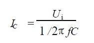
Where Ui --- input AC voltage rms value.
f---AC signal frequency.
Therefore, for the 64 mA current IO consumed by the load, at least the buck capacitor value C min = 0. 928 μF. In addition, in order to ensure reliable operation of C, the withstand voltage should be greater than 2 times the supply voltage. Therefore, select two A 684MF / 630 V capacitor works in parallel.
1. 2. 2 output rectification and filter circuit
According to some literatures, the maximum voltage U RM = √2Ui (Ui is the effective value of the input voltage) of a single diode on the rectifier bridge = 318. 4 V, therefore, the commonly used rectifier diode 1N4007 (U RM = 1000 V, I F = 1 A).
In order to obtain a smooth load voltage at the output, R L C ≥ (3~5) T /2 is generally taken, where RL is the load impedance and T is the input signal period (0. 02 s), and C ≥ 24.38 is obtained. μF. In principle, the larger the capacitance value is, the smoother the output voltage is, and the smaller the ripple value is. However, as the capacitance increases, its volume also increases. Considering that the circuit should be installed in a common T8 tube, take 33μF / 160V electrolytic capacitor; at the same time, to obtain a smoother output voltage, select L1 is a 100 μH wirewound inductor, and C1 is a 0.01 μF ceramic capacitor.
1. 2. 3 output protection circuit design
The current used in the LED can't exceed the stable value of the specification. The long-term overload will not increase the brightness (the white LED will saturate at high current, the luminous efficiency will be greatly reduced), and it will shorten the LED life and affect the LED lighting. Circuit reliability. Since the LED's forward voltage is small, the small change of the forward voltage will cause a large change in the LED current. Therefore, an output protection circuit needs to be provided at the output.
The circuit consists of VT1, R 2 and R 3 . VT1 uses Motoro2la's MCR729210 (U DRM = 800 V, gate trigger voltage U GT = 0.8 V, trigger current I GT = 10 mA). R2 is one-way. The thyristor provides a trigger bias voltage, and the selection of its resistance value is very important. If the value is too large, some unstable factors in the circuit cause the current in the LED to become instantaneously large, which causes the thyristor to be frequently triggered, and the protection circuit frequently acts. The circuit is not working properly; if the resistance value is too small, the LED may work beyond its stable value, and the protection circuit is insensitive, which will shorten the LED life. Since the LED branch current is required to be 16 mA, then:
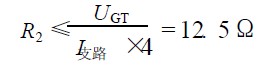
To leave a certain margin, choose R2 = 10Ω.
2 Simulation and experimental analysis
2. 1 PSpice simulation of fluorescent lamp circuit
In order to verify the feasibility of the design in theory, the circuit was simulated by PSp ice software. The result is shown in Figure 2. The circuit enters a steady state at 210 ms. After stabilization, its output voltage is 97 ± 2. 2 V, and the output current is 14. 7 ± 0.3 mA, which basically verifies the feasibility of the circuit design. The output characteristics of the LED fluorescent lamp circuit are shown in Figure 2.
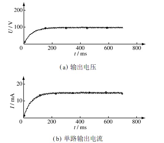
Figure 2 LED fluorescent lamp output characteristics.
In order to verify the function of the output protection circuit, the parameter R1 is subjected to parameter scan analysis, and then performance analysis is performed. The result is shown in Figure 3. It can be seen that when R2 increases from 1 Ω to 13.889Ω, the output current begins to decrease, indicating that the unidirectional thyristor is in a critical conduction state; then as R2 continues to increase, the output current drops sharply until R2 At 15.119 Ω, the output current is stable at about 5.2 mA, indicating that the unidirectional thyristor is fully turned on and the protection circuit is active.
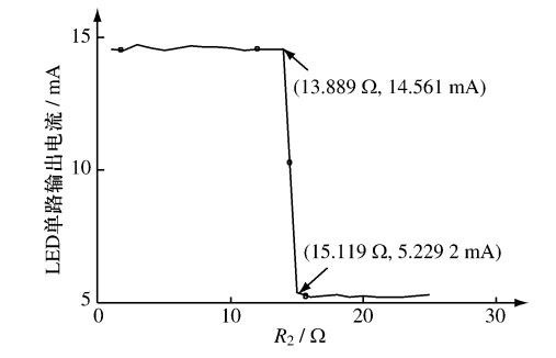
Figure 3 output current and R2 resistance curve
2. 2 test data
From the results of the PSp ice simulation, the circuit design is feasible, so 12 W fluorescent lamps were fabricated according to this circuit. The standard lamp is 1 190 mm × 30 mm, which is made up of two identical PCB boards (size 593 mm × 25 mm). The relevant parameters of the circuit are analyzed by Huzhou CSR SPL2000 electric light source color and color comprehensive analysis system. taking the test. When the measured input voltage VAC is 220 V, the total current of the circuit is 127 mA, which is equivalent to 15.85 mA per branch, the power factor of the circuit is 0. 465, and the power consumption of the circuit is 11.4W.
Tested without damaging the LED, the relationship between the capacitance of the step-down capacitor C1 and the output current is shown in Figure 4 (since the two capacitors are identical, only a single capacitor value is shown in Figure 4). It can be seen that as the capacitance value increases, the output current rises almost linearly. When it is increased to a certain value (about 20 mA), the protection circuit acts to force the current through the LED branch to drop.
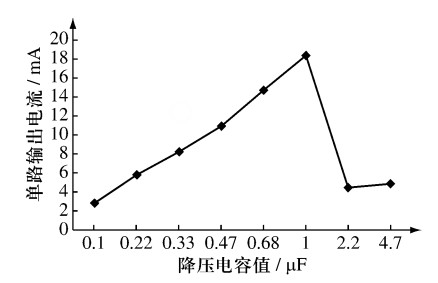
Figure 4 shows the relationship between measured output current and step-down capacitor
3 Conclusion
A 12 W standard T8 LED fluorescent lamp circuit is designed using a capacitive buck drive circuit. The circuit has the characteristics of small size, low cost, etc., and can be suitably used as a power source for various LED lamps by changing the step-down capacitor. Although the power factor of the power supply is low, it is especially suitable for low-end lighting market applications. According to this circuit, a variety of lighting products such as 1W, 4W, 8 W, and 12 W were produced by changing the value of the step-down capacitor.
Aluminium Led Channel Letter,Led Aluminum Channel Signs,Custom Channel Letter Signs,Led Backlit Aluminum Channel Letters
Wuxi Motian Signage Co., Ltd , https://www.makesignage.com