In the LED packaging process, electrode contamination often occurs after solid crystal baking. In this paper, the pollutants were analyzed and the contaminants were found to be solid oxide gel volatiles. On this basis, two possible reasons for the adhesion of the die-bonded chip electrodes were analyzed, and the corresponding solutions were given.
One electrode contamination
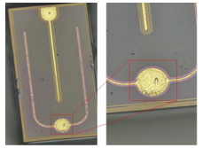
At present, in the LED packaging process, after the solid crystal glue is baked and solidified, contaminants adhere to the gold electrode, resulting in insufficient wire bonding or insufficient wire drawing force.
As shown on the right, a metallographic microscope was used to observe significant contaminants on the electrodes.
Two reasons analysis and solution
1 Contaminant composition
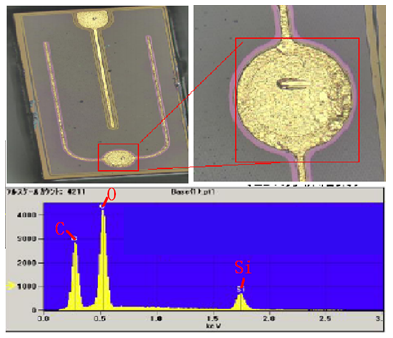
As shown in the figure, an electronic energy spectrometer (EDS, Energy Dispersive Spectrometer, which can analyze the type and content of the constituent elements in the micro-area of ​​the material) is used to perform elemental analysis on the contaminated part of the chip, and the C, O, and Si elements are detected, and the solid crystal glue is detected. The main component is siloxane (element is H, C, O, Si). Since EDS cannot detect H element, it can be inferred that the chip electrode contaminant contains a solid crystal glue component.
2 Cause analysis
Through elemental analysis, we speculate that the contaminant is a solid crystal glue, indicating that the solid crystal glue and the electrode have some combination during baking.
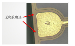
The solid glue can be contacted with the electrode by volatilization and creeping. However, it can be seen from the photomicrograph analysis that there is no trace of creeping around the chip, so it is possible to eliminate the possibility of chip contamination caused by the solid crystal glue, while the solid glue will have a small amount of volatiles during the curing process. The small molecule cross-linking agent with hydroxyl group contained in the product has high chemical activity and is likely to be the main cause of adsorption pollution.
So how does the solid oxide gel volatiles adsorb to the chip electrodes? We made the following two speculations:
1. Hydroxyl small molecule cross-linking agent and chemical adsorption of chip electrode contaminants
Since the crosslinking agent itself does not react with the gold electrode, and there is a possibility of residual active contaminants in the production process of the chip, it is speculated that the crosslinking agent may chemically react with the residual pollutants in the electrode preparation process to cause adsorption.
2. Static adsorption of the hydroxyl-containing small molecule cross-linking agent and the chip electrode
Since the oxygen atom in the hydroxyl group is relatively electronegative, the common electron between the hydrogen and the oxygen is shifted toward the oxygen atom, and the positive and negative electric centers are not in the equilibrium position, so that the molecular susceptibility is obtained. The person will generate electrostatic attraction and then adsorb together to form pollution.
2.1 Hydroxyl small molecule cross-linking agent and chemical adsorption of chip electrode contaminants
2.1.1 Source of chip contaminants
The contamination of the chip may be due to contamination introduced during the chip manufacturing process and contamination introduced during the die bonding operation (such as touching the chip during operation).
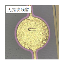
We observed the chip on which the electrode was stained by a microscope, and no traces of contamination (such as fingerprints) were observed on the surface, so that chip contamination due to manual operation can be eliminated.
In the preparation process of the chip, multiple photolithography is required, and the photolithography involves the development process. Currently, the commonly used developer is an inorganic alkali + hydrogen peroxide solution (such as sodium carbonate solution), which will leave residual hydroxyl groups on the surface of the chip electrode. Functional group. In the subsequent process, the chip manufacturer will add chemical cleaning and water washing steps to clean the attached ionic contamination, but there may be secondary cleaning caused by incomplete cleaning or improper maintenance of the cleaning equipment.

As shown in the photolithography and development process, after the photoresist is exposed to ultraviolet light through the mask, and then washed by the developer, a pattern corresponding to the mask is left, and the process becomes "graphics." "," is the necessary process to make the three-dimensional structure of the chip.
2.1.2 Source of solid crystal glue volatiles
The small molecule cross-linking agent with hydroxyl group in the solid crystal glue has a short molecular chain and a low boiling point. It volatilizes without participating in the reaction during heating and solidification, and contains hydroxyl groups and residual hydroxyl groups on the gold electrode through hydrogen and oxygen. The hydrogen bonds between them are adsorbed together, and then a further chemical reaction takes place.
What is a hydrogen bond?
The hydrogen bond means that a hydrogen atom is covalently bonded to an atom X (O, F, N, etc.) having a large electronegativity, and is close to an atom Y (O, F, N, etc.) having a large electronegativity and a small radius. , a hydrogen-mediated medium between X and Y, produces a special intermolecular or intramolecular interaction in the form of XH...Y, called a hydrogen bond.

2.1.3 Reaction process
As shown in the figure, when the hydroxyl group-containing small molecule crosslinker volatilized in the solid crystal glue contacts the hydroxyl group remaining on the surface of the electrode, the oxygen atom on the hydroxyl group generates a hydrogen bond with the hydrogen on the other hydroxyl group, and the same pair of hydrogen And the oxygen atom also forms a hydrogen bond.
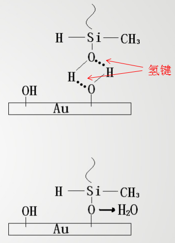
Then some of the hydrogen bonds are converted into covalent bonds and one water molecule is removed. The generated water molecules are discharged with hot air in the oven under high temperature baking. As time goes on, more and more crosslinkers react with residual hydroxyl groups. Finally, the surface of the chip leaves a large amount of solid crystal adhesive containing C, O, Si elements.
2.1.4 Experimental verification
The chip confirmed to be clean and free of electrode contamination was fixed on the substrate as shown, and divided into A and B; 1 A was soaked in an alkaline solution (sodium carbonate solution) for 3 minutes, and then dried with nitrogen; 2 B was left untreated.
Then apply the same amount of solid crystal glue around the chips of A and B respectively, then cover A and B with a beaker as shown in the figure and bake in the oven (120 ° C / 1H + 160 ° C / 2H).
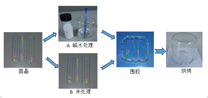
After the baking was completed, the electrode portions of the chips of A and B were observed with a metallographic microscope, and the results are as follows:

Note: The picture is taken in dark field, the black area is the electrode metal layer; the chip test point is the trace left during the chip lighting test.
It can be clearly seen from the figure that after the lye immersion treatment, a large amount of contaminants adhere to the surface of the electrode after the solid crystal baking, and the untreated clean chip has substantially no contaminants.
It is indicated that the reactive groups such as hydroxyl groups remaining on the surface of the electrode react with the volatiles of the solid crystal glue to cause adhesion of the solid crystal glue on the surface of the electrode.
2.1.5 Solution
After the above experiments, we can confirm that the pollution is mainly due to the chemical reaction between the reactive groups such as hydroxyl groups remaining in the preparation process of the chip and the volatile hydroxyl group-containing small molecule crosslinkers in the solid crystal glue. To solve such pollution, We need to improve from both the chip and the solid crystal glue.
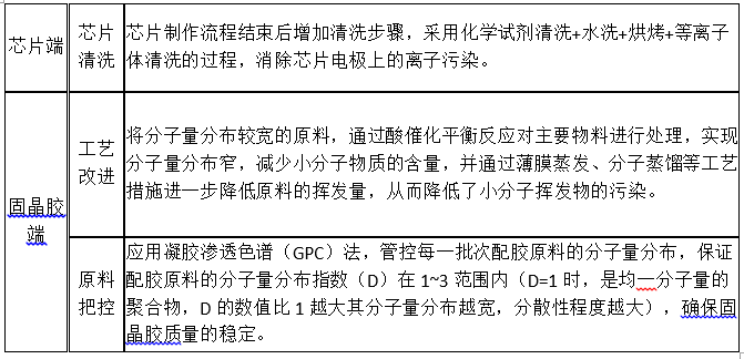
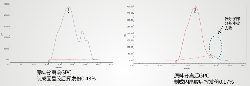
As shown in the figure, after the separation of small molecular substances in the solid-crystal collagen material by thin film evaporation, molecular distillation and other process measures, it can be seen from the GPC test results that the uniformity of the molecular weight distribution of the solid crystal glue is greatly improved. The volatile content decreased from 0.48% to 0.17%, which greatly reduced the amount of volatilization. It shows that through the technical improvement and raw material control of the solid crystal glue manufacturer, it can effectively reduce the volatile matter of the solid crystal glue and reduce the electrode pollution.
2.2 Hydroxyl group-containing small molecule cross-linking agent and electrostatically adsorbed on the chip electrode
2.2.1 Causes of chip charging
The chip is adhered to the blue film. It needs to be peeled off to expand the crystal during use. This process is easy to generate static electricity. The standard operating procedure (SOP) stipulates that the crystal expansion station needs to be equipped with an ion fan and the ion fan. The air outlet is subjected to tearing blue film and crystal expansion operation, and the operator needs to wear an electrostatic wristband to prevent static electricity generated by the chip. However, some operators in the actual production do not operate according to the regulations, and the ion fan is not used, which may cause the chip to be charged.
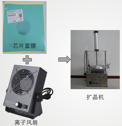
Correct operation process: wear an electrostatic wristband, tear the blue film under the ion fan, and then use the crystal expander to expand the crystal.
2.2.2 Electrostatic adsorption mechanism
Since the solid crystal glue contains a small molecule cross-linking agent with a hydroxyl group, the molecular chain is short, the boiling point is low, and it is easily volatilized during heating and solidification, and a trace amount of silica gel component is attached.
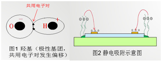
As shown in Fig. 1, the hydroxyl group contained in the cross-linking agent is a strong polar group, and its oxygen atom is highly electronegative, so that the common electron opposite oxygen atom between hydrogen and oxygen is shifted, and the positive and negative electric centers are not. Equilibrium position, making the group externally responsive;
If the electrode of the chip is charged, these polar groups will form an electrophoresis phenomenon in the air and be concentrated at the electrode point by electrostatic adsorption; as shown in Figure 2, these enrichments (small molecule crosslinkers and attached traces) The silica gel component is deposited on the surface of the electrode, and the trace amount of silica gel contained in the baking process is solidified by the cross-linking agent, and a large amount of unreacted cross-linking agent forms a liquid-like contaminant remaining on the surface of the chip electrode due to enrichment. . Since the electrode dots are blocked by these organic substances, the gold wire or the alloy wire cannot be soldered normally at the electrode dots.
2.2.3 Experimental verification
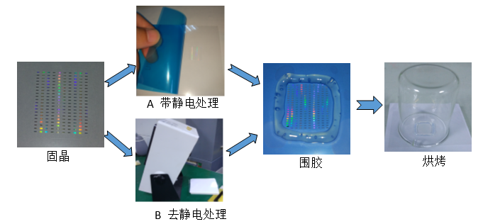
The chip is fixed on the substrate as shown, divided into A and B; 1 The A chip is covered with a blue film, and then the chip is charged by tearing the blue film; 2 B is blown under the ion fan for 20 minutes. , completely eliminate the static electricity carried by the chip.
Then apply the same amount of solid crystal glue around the chips of A and B respectively, then cover A and B with a beaker as shown in the figure and bake in the oven (120 ° C / 1H + 160 ° C / 2H).
After the baking was completed, the electrode portions of the chips of A and B were observed with a metallographic microscope, and the results are as follows:

Note: The picture is taken in dark field, the black area is the electrode metal layer; the chip test point is the trace left during the chip lighting test.
It can be clearly seen from the figure that after electrostatic treatment, a large amount of contaminants adhere to the surface of the electrode after solid crystal baking; and the chip removed by static electricity has substantially no contaminants.
It indicates that the charging of the chip will cause electrostatic attraction of the solid oxide volatilizer and the electrode during baking, which will cause the solid glue to be concentrated and contaminated on the electrode surface.
2.2.4 Solution
After the above analysis, we can confirm that the pollution is mainly caused by the abnormal operation of the chip electrode during the use of the chip, and the electrostatic adsorption of the hydroxyl-containing small molecule cross-linking agent and the electrode which are volatilized in the solid crystal glue To solve such pollution, we need to improve both the operating specifications and the solid crystal glue.

Three summary
After the above analysis, we can know that the contaminant attached to the chip electrode after the solid crystal baking in the LED packaging process is a solid crystal glue. The hydroxyl group-containing small molecule cross-linking agent which is volatilized during the baking of the solid crystal glue is adsorbed to the electrode by two reasons: 1 the hydroxyl group-containing small molecule cross-linking agent is chemically adsorbed with the chip electrode contaminant; 2 the hydroxyl group-containing small molecule cross-linking Electrostatic adsorption of the agent and the chip electrode; through experimental verification we can see that the degree of contamination of the chip treated by alkaline water is much greater than that of the chip with electrostatic treatment, so we push chemical adsorption as the main reason, electrostatic adsorption is a secondary cause. For the above two reasons, we have the following solutions:

references:
Liu Xing. Mechanism of silane molecule adsorption and film formation kinetics on metal surface [D]. China University of Geosciences (Wuhan), 2012.
Geng Yiping, Tang Bing, Huang Shuhuan. Advances in Adsorption of Organic Substances on Metal Surfaces[J].Surface Technology, 2009, 38(2):70-72.
Author: Fang Huayu, Pei Xiaoming

In many electronic communication equipment and instruments where always use some cable assemblies to connect some electronic units and circuits. Xi'an KNT Scien-tech can use their technology, euqipment, skilled operation, advanced test equipment and method (IEC 9661-4). different connnectors (SMA, SMB, N, TNC, etc. ) and different cables (FLExible cable, semi-flexible cable, Semi-rigid cable, corrugated cable etc.) to offer customer various reasonable price cable assemblies fully with the customer requirements.
SMA cable
Xi'an KNT Scien-tech Co., Ltd , https://www.honorconnector.com