With the development of measurement and control technology, the measurement control network composed of multiple single-chip microcomputers is more and more widely used in the field of measurement and control. The data exchange between the MCUs usually adopts the serial communication mode, and the connection mode mostly adopts the bus topology [13]. In the structure, the single-chip microcomputer is connected through a set of data lines, and all the single-chip microcomputers share a set of data lines; when communicating, the slave MCU is addressed, and the main MCU accesses the slave MCU through different addresses. Since there is only one set of data lines, the master MCU can only communicate with one MCU at the same time. If you want to access the slave microcontroller once, then the master microcontroller must first send an access command from the microcontroller, and wait for its response before accessing the next slave microcontroller. This wastes a lot of time and reduces the efficiency of the measurement and control system. In some supervised computer control systems (SCC) and distributed control systems (DCS) [4], the main MCU often needs to access the slave MCU at the same time, requiring the MCU to respond to the access command of the MCU at the same time. At this time, the topology bus structure Can not meet the requirements.
With the development of electronic technology and EDA technology, FPGA technology has become more and more widely used in the field of electronic design with its unique advantages. FPGAs offer the advantages of high integration, small size, and low power consumption, as well as user-programmability. The use of FPGA devices can greatly shorten the development cycle, reduce capital investment, and realize the design of on-chip programmable system (SOPC). At the same time, the trend of using serial extended communication in measurement and control systems is becoming more and more prominent, but the lower response efficiency of traditional bus topology can not meet the requirements of complex systems. The main purpose of this paper is to design a module based on FPGA that integrates 16 simple UARTs (Universal Asynchronous Receiver and Transmitter), which is described in VHDL language. The main MCU is connected to the FPGA through the parallel port, and the FPGA is connected to the 16 MCUs through 16 UARTs respectively to realize the serial communication network system of the MCU.
1 system hardware overall design The system design requires that the main MCU can simultaneously control the slave MCU, and can simultaneously collect the information uploaded from the MCU, judge it and transmit it to the host computer. The main MCU functions are:
1 Communicate with the host computer, receive the host computer command and parse it;
2 According to the command of the host computer, control the slave microcontroller downwards;
3 Monitor whether the various indicators uploaded from the MCU meet the requirements;
4 Provide an alarm display.
The FPGA completes the demultiplexing of the main MCU command and the multiplexing of the information uploaded from the MCU. The main function of the MCU is to receive the command sent by the host MCU through the FPGA, complete the control of the device and upload the device status, as shown in Figure 1.
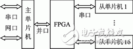
Figure 1 Schematic diagram of multi-computer communication principle of single-chip microcomputer
The single chip used in this design is Cygnal's C8051F series MCU, and the FPGA is Xilinx's XC3S100E. C8051F series MCU is a high-end MCU developed by Cygnal. The instruction is compatible with 8051. It has a processing capacity of up to 25 MIPS. It also integrates a wide range of peripherals such as ADC, DAC, programmable amplifier, voltage comparator and sensor. It is very suitable for application. The field of measurement and control. The C8051F series MCU also has a JTAG interface, which is convenient for users to debug online, which greatly saves the user's development time.
2 system implementation 2.1 main microcontroller unit designThe main single chip adopts C8051F020 single chip microcomputer. The single chip provides two serial ports and one I2C interface (SMBus), and provides parallel ports of P0~P3 or P4~P7. In this design, the special function register EMI0CF=0x27 is set to make the external memory interface work in the address/data multiplexing mode, and the high port P4~P7 is selected. Set the special function register XBR0=0x15 to map the serial port UART0 and SMBus to the P0 port.
The C8051F020 treats the FPGA as an external memory and accesses it through the parallel ports P4~P7. The C8051F020 connects the serial EEPROM through the SMBus interface, writes the system information to the EEPROM in real time, and reads the data in the EEPROM when the system is suddenly powered off, and completes the system power-down protection function. The main MCU continuously analyzes the commands uploaded from the MCU continuously, judges the status of the device and gives an alarm display, and simultaneously stores it in the internal buffer to wait for the upper computer to query.
The C8051F020 provides serial port and network port two ways to communicate with the host computer. The two interfaces cannot be used at the same time. The network communication is realized by the network port serial port conversion module. The network port and the serial port are connected to the UART0 of the C8051F020 through a combination logic circuit, as shown in FIG. 2, and the local monitoring and remote monitoring functions of the system are realized.
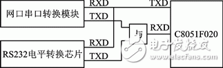
Figure 2 Schematic diagram of the serial port and network port connection of the main MCU
2.2 FPGA unit designThe design of the FPGA is a core part of the communication network. According to the functional requirements, the FPGA is divided into four major functional modules: SRAM controller, transmit data buffer module, 16 UART modules, and receive data buffer module. The transmit data buffer module is divided into 16 RAM areas, and each RAM area is respectively connected with one UART. When the transmit buffer module receives the control data sent by the host microcontroller, the UART is started to send data to the slave microcontroller. The receive buffer is also divided into 16 RAM areas. After transmitting the control data, the UART periodically sends a status inquiry command to the slave microcontroller, and the latest status is sent from the microcontroller to the UART module. The UART module stores the data in the corresponding RAM of the receive buffer module. Area. As shown in Figure 3.
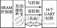
Figure 3 Schematic diagram of the internal function block of the FPGA
There are 16 pairs of read/write and data buses inside the FPGA, which are connected to the UART and the corresponding transmit buffer RAM and receive buffer RAM respectively.
Guangzhou Bolei Electronic Technology Co., Ltd. , https://www.nzpal.com