MicroLED is a new generation display technology that offers higher brightness, better luminous efficiency, and lower power consumption than existing OLED technologies. In May 2017, Apple has begun the development of a new generation of display technology. In February 2018, Samsung introduced the MicroLED TV on the CES2018.
Micro LED featuresMicroLEDs offer higher brightness, better luminous efficiency, and lower power consumption than existing OLED technologies. The outstanding features of microLED will make it available on TV, iPhone, iPad.
Speaking of Micro LED, we must start with the application of TFT-LCD backlight module. In the 1990s, when TFT-LCD began to flourish, some manufacturers used LEDs as backlights because of their high color saturation, power saving, and thinness. However, due to factors such as high cost, poor heat dissipation, and low photoelectric efficiency, it has not been widely used in TFT-LCD products.
Until 2000, the process, performance and cost of blue LED chips stimulating phosphors to make white LED technology began to mature. When it entered 2008, white LED backlight modules showed explosive growth, and almost completely replaced CCFL in a few years. Applications range from mobile phones, tablets, laptops, desktop monitors to televisions.
However, due to the display principle of TFT-LCD non-self-luminous, the open cell transmittance is less than 7%, which causes the photoelectric efficiency of TFT-LCD to be low; and the color saturation of white LEDs is still not as good as the three primary colors. Most TFT-LCD products are only about 72% NTSC; in addition, in outdoor environments, TFT-LCD brightness cannot be increased to more than 1000 nits, resulting in low image and color recognition, which is a major application defect. Therefore, another technology that directly uses the three primary color LEDs as the LED display or the Micro LED Display of the self-luminous display dot pixels is also under development.
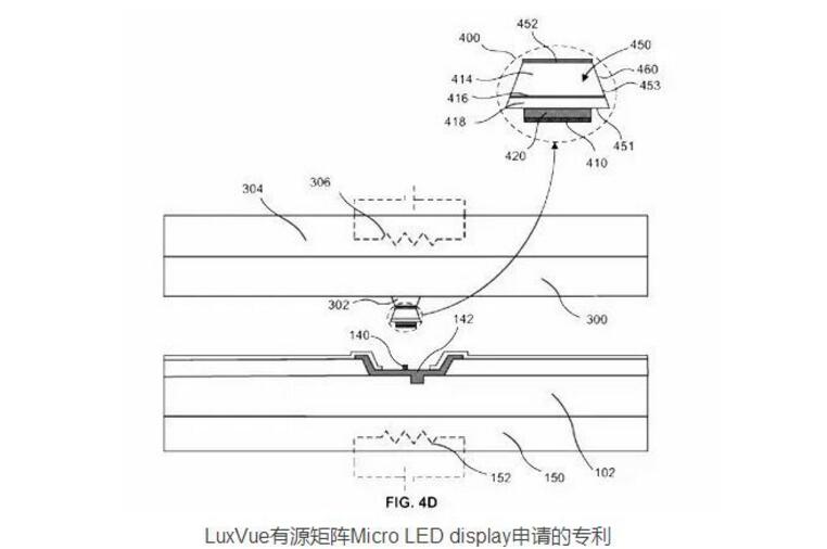
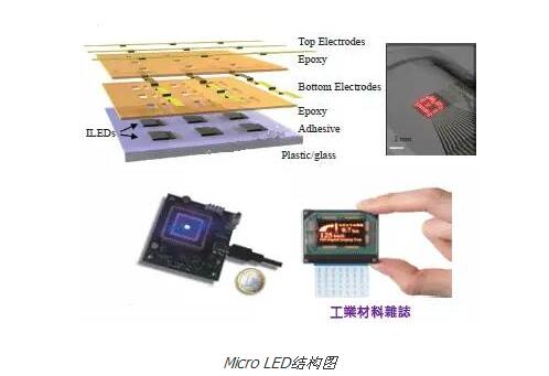
The display principle of MicroLEDDisplay is to thin, miniaturize and array the LED structure design, and its size is only about 1~10μm. After that, the MicroLED is transferred to the circuit board in batches, and the substrate can be hard and soft. On the transparent and opaque substrate; the protective layer and the upper electrode are completed by a physical deposition process, and the upper substrate can be packaged to complete a simple microLED display.
To make a display, the surface of the wafer must be made into an array structure like an LED display, and each dot pixel must be addressable and individually driven to illuminate. If driven by a complementary metal-oxide-semiconductor circuit, it is an active addressing drive architecture, and the micro-LED array chip and CMOS can be packaged.
After the bonding is completed, the MicroLED can improve brightness and contrast by integrating the microlens array. The microLED array connects the positive and negative poles of each MicroLED via vertically interleaved positive and negative grid electrodes, sequentially energizes through the electrode lines, and illuminates the MicroLEDs by scanning to display images.
A typical structure of a MicroLED is a PN junction diode composed of a direct energy gap semiconductor material. When a forward bias is applied to the upper and lower electrodes of the MicroLED to cause the current to pass, the electrons and holes recombine with respect to the active region, and a single color light is emitted. The FWHM of the main wavelength of the MicroLED spectrum is about 20 nm, which provides extremely high color saturation, usually 120% NTSC.
Moreover, since 2008, LED photoelectric conversion efficiency has been greatly improved, and 100 lm/W or more has become a mass production standard. Therefore, for the application of the MicroLED display, the low-energy or high-brightness display design can be easily realized due to its self-illuminating display characteristics and a simple structure with almost no light-consuming components.
This can solve the two major problems of current display applications. First, more than 80% of the energy consumption of wearable devices, mobile phones, tablets and other devices is on the display, low-energy display technology can provide longer battery life; second, ambient light Stronger causes the image on the display to be whitened and the recognition is worse. The high-brightness display technology can make the application scope wider.
Micro LED advantageHigh brightness, low power consumption, ultra high resolution and color saturation. MicrolED's biggest advantage comes from its biggest feature, micron-level spacing, pixel positioning for each pixel and single-point drive illumination. Compared with other LEDs, the luminous efficiency is currently the highest, and the space is still greatly increased; the luminous energy density, the MICROLED is the highest, and there is room for improvement. ——The former is beneficial to the energy saving of display devices. Its power consumption is about 10% of LCD and 50% of OLED. The latter can save the limited surface area of ​​display devices and deploy more sensors. The current theoretical result is Compared with OLEDD, MICROLED and OLEDD achieve the same display brightness, only about 10% of the coated area of ​​the latter. Compared with OLEDs, which are also self-luminous displays, the brightness is 30 times higher and the resolution is up to 1500 PPI (pixel density), which is equivalent to 5 times that of AppleWatch using OLED panels up to 300 PPI.
long life. Because Micro-LED uses inorganic materials, and its structure is simple, it has almost no light consumption, and its service life is very long. This is incomparable to OLEDs. OLEDs, as organic materials and organic substances, have inherent defects - life and stability - that are difficult to match the QLEDs and MICROLEDs of inorganic materials.
Can adapt to a variety of sizes.
The cost reduction space is large. At present, the micro-projection technology mainly uses Digital Light Processing (DLP), Reflective Silicon Substrate Liquid Crystal Display (LCOS), and Micro Electro Mechanical System Scanning (MEMSScanning) technology, but all of these technologies require the use of an external light source. The module volume is not easy to be further reduced, and the cost is also high. In contrast, the self-illuminating MicroLED microdisplay does not require an external light source, and the optical system is relatively simple, so it has an advantage in miniaturization and cost reduction of the module.
Wide range of applications. MicroLED solves several major problems. One is that consumer tablets include smartphones, and wearable devices consume 80% of the energy on the display. Low-energy MicroLED displays will greatly extend battery life. For MicroLED display applications, The display characteristics of the light, combined with the simple structure of almost no light-consuming components, can easily achieve low-energy or high-brightness display design. Second, the strong ambient light causes the image on the display to be whitened and the recognition degree is deteriorated. MicroLED's high-brightness display technology can easily solve this problem and make its application scope wider.
For a MicroLED display product, his basic components are TFT substrate, ultra-light LED die, and driver IC. These three have a common feature, that is, a large number of inherited from the existing LCD and LED industries. Therefore, the Taiwan Industrial Technology Research Institute believes that they have the advantages of the entire industrial chain.
However, regions with the same industrial base include South Korea, mainland China, and Japan. Among them, Japan's leading and perfection in upstream materials and equipment far exceeds that of Taiwan. However, the interest of Japanese colleagues in MicroLED is not as high as that of the Taiwanese industry.
Why are other regions with comparable or better industrial bases less enthusiasm for MicroLED than Taiwan? The answer is divided into two levels: The first is that the mainland, South Korea and Japan show the business, and now the busiest thing is OLED. Second, MicroLED has a highly difficult process that is rarely used in other electronics industries – massive micro-transfers (also called massive transfers). One of the biggest moves in Taiwan's MicroLED industry was the establishment of the “Big Micro-Transfer†industry alliance in December 2016 with the Taiwan Industrial Technology Research Institute as the lead unit.
What is the technology of “huge transfer� Simply put, on the TFT circuit board of the fingernail size, according to the optical and electrical specifications, evenly solder three or five hundred, or even more, red, green and blue primary color LED micro-die, and the allowable process failure rate is several One in ten thousand. - Only products that achieve such a process can be truly applied to products such as AppleWatch3.
For the process problems of MicroLED, many people think that they can take experience from traditional LED screens. However, MicroLED differs greatly from traditional LED display products. Compared with traditional LED display, the difference between MicroLED is mainly: 1. Tens of times the precision is improved; 2. The integration process has changed from "in-line, surface mount, COB package, etc." to "macro-micro transfer"; The defect repairability is almost zero; 4. The backplane is changed from a printed circuit board to a TFT substrate used for liquid crystal and OLED display, or a single crystal silicon substrate used for a CPU and a memory.
That is to say, compared with the traditional LED display, MicroLED is different in every aspect of die, package, integration process, backplane, drive, etc. - so, you can see that the heat of MicroLED products has not been obtained by any traditional LED large-screen manufacturer. Statement.
In fact, in addition to the "meta-group" of die, TFT backplane, IC, inherited from LED die (such as Sanan), semiconductor display (such as BOE), IC design companies (such as accumulation, wonders), etc. The core of MicroLED is really "how to integrate these components", that is, "huge transfer" technology. The latter is the lifeblood of the entire industry. If a company wants to take the lead in MicroLED products, the most needed is to start from here.
In this regard, the more accurate news is: In February of this year, MikroMesa and Chongqing Huike jointly created the cooperation of the first MicroLED panel laboratory on both sides of the strait. The lab is scheduled to be completed by the end of this year and will produce full-color MicroLED samples in 2018. MikroMesa currently has leading R&D technology on LED micro-grains and is rumored to be 3UM. Huike has built A-SILCD production line and has technical resources such as TFT backplane. The purpose of the cooperation between the two is to use the resources that are likely to be ready to break through the “huge transfer†technology.
However, even this relatively in-depth project is not optimistic about MicroLED's industry timeline: it is still difficult to say how far it will be from real business applications in 2018. Taking OLED as an example, it has achieved full color, and the large-scale recognition of the mobile phone industry has gone on for more than 20 years. Moreover, Huike and MikroMesa are newcomers to the display circle. Both of them pay attention to the intention of MicroLED to attempt to overtake the curve.
In summary, from the component point of view, MicroLED is not difficult on TFT, IC, LED die; but from the perspective of process and industrial process, the huge amount of transfer between the vision and reality of MicroLED is difficult to completely cross in the short term.
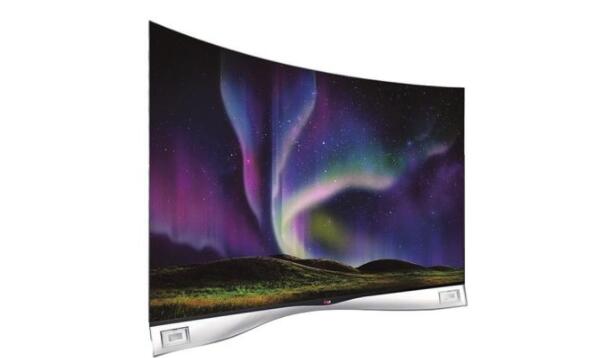
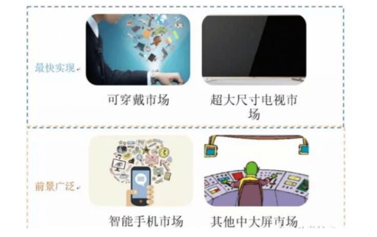
Micro LED applications have broad prospectsAt present, if you consider the existing technical capabilities, Micro-LED has two major application directions. One is the wearable market, represented by Apple. It is said that Apple will use Micro-LED technology on a new generation of Apple Watches and iPhones, and is expected to The Micro LED wearable device was introduced in 2018. Second, the oversized TV market, represented by Sony, this year, Sony's Micro-LED cledis demonstrated at CES has excellent performance in resolution, brightness and contrast.
In the short term, the Micro-LED market is concentrated on ultra-small displays. In the medium and long term, Micro-LEDs are used in a wide range of applications, including wearable devices, large indoor display screens, head-mounted displays (HUD), and head-up displays. (HUD), taillights, wireless optical communication Li-Fi, AR/VR, projectors and many other fields.
VEIIK Ticko Vape Series are so convenient, portable, and small volume, you just need to take them out of your pocket and take a puff, feel the cloud
of smoke, and the fragrance of fruit surrounding you. It's so great.
We are the distributor of the VEIIK Vape brand, we sell veiik e cigarette, veiik vape pen, veiik disposable vaporizer, and so on.
We are also China's leading manufacturer and supplier of Disposable Vapes puff bars, disposable vape kit, e-cigarette, vape pens, and e-cigarette kit,
and we specialize in disposable vapes, e-cigarette vape pens, e-cigarette kits, etc.
veiik ticko vape bar,veiik ticko vape starter kit,veiik ticko vape device,veiik ticko vape pen,veiik ticko vape disposable
Ningbo Autrends International Trade Co.,Ltd. , https://www.ecigarettevapepods.com