The physical interference of dc/dc switching power converters is well known unless the system and circuit diagrams are carefully designed. These converters can inject extra charge electrically, producing spurious digital signals, flipping double clocks, electromagnetic interference, analog voltage errors, and potentially high voltages. With the increasing complexity of such designs and the intensive use of applications, the implementation of physical circuits has begun to play an important role in the electrical integrity of the system. To solve these problems, you need to understand how to reduce the two main types of ground noise sources.
Ground noise problem oneFigure 1 shows an ideal buck converter with a constant load current. Switches S1 and S2 are switched back and forth to interrupt the input voltage on the buck inductor and buck capacitor. The inductor current or capacitor voltage cannot be changed abruptly, and the load current is constant. All switching voltages and currents should successfully cross the buck inductor or pass the buck capacitor, respectively, because an ideal buck converter will not generate ground noise. But experienced designers know that buck converters are a notorious source of noise. This means that the circuit in Figure 1 lacks some key physical components.
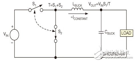
In Figure 1, in a buck converter circuit, the current of the inductor cannot be changed instantaneously, so it is difficult to determine the ground bounce source in an ideal buck converter.
Whenever there is a charge movement, a magnetic field is generated. A wire, a resistor, a transistor, a superconductor, or a current between a capacitor plate produces a magnetic field. The magnetic flux is the magnetic induction intensity through a current loop area, which is equal to the product of the magnetic induction intensity of the loop area cut at right angles and the loop area: φB = B & TImes; A, where φB is the magnetic flux, B is the magnetic induction, and A is the current Loop area. The magnetic induction around a wire at a distance is proportional to the current in the wire, B = μoI / 2πr, where r is the distance.
Electronic components have lengths that must travel along one wire segment from one device to another. The moving charge creates a magnetic field, so we can improve the circuit in Figure 1. Figure 2 is a better model of a simple buck converter. In Figure 2, the wires remain ideal, but current must flow a distance in each segment as it moves from one electronic component to another. When this charge flows, the magnetic field surrounds the energized wire and the magnetic flux passes through the cycle of the S1 and S2 switches.
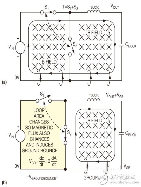
Figure 2, the varying flux produces a voltage (a). When a buck is switched, the varying current loop path produces a varying flux and causes the ground bounce (b).
The change in the area of ​​the S1 and S2 current loops is the first major source of noise in the switching converter. During each switching cycle, the magnetic flux in this loop of the input voltage -S1-ground increases and decays. This varying flux induces voltage across the loop, including the ideal ground return line. No copper foil (even a superconductor) can eliminate this induced voltage. The only useful method is to reduce the varying flux.
The changing flux has three major factors: rate of change, magnetic field strength, and loop area. Since the clock frequency and maximum output current may have design requirements, it is best to minimize the loop area. The inductance is proportional to the magnetic flux.
3 is an electrical model of FIG. 2 in which a change in current in parasitic inductance LP1 produces ground noise, while a constant current in parasitic inductance LP2 does not contribute. Although Figure 3 illustrates the problem in a similar manner, it is a poor alternative to the physical enhancement model of Figure 2. Figure 3 shows the parasitic induced voltages on LP1 and LP2, which induce voltage across a loop with flux changes. However, this circuit component can still be used to demonstrate how to reduce the induced ground noise.
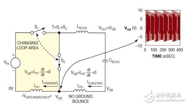
In Figure 3, the varying current in LP1 produces a ground bounce, while the constant current in LP2 does not.
In Figure 3, the ground loop current flows through LP1 and changes, which creates a voltage bounce problem. Careful placement of the input capacitor reduces the parasitic flux area and allows the varying step-down current to go through a path that is not included in the ground return (Figure 4). At this time, the currents in the parasitic inductances LP1 and LP2 are constant, and thus the ground voltage is stable. The reduction in flux area also proportionally reduces EMI, as well as all other unwanted inductive loop voltages.
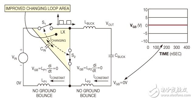
Figure 4. Carefully lay the input capacitors, minimize the area of ​​the changing loop, and carefully lay out the changing current path of the ground loop to eliminate ground bounce.
The first important source of grounding noise for switching converters is the result of changing flux areas. A good PCB design minimizes the varying current loop area and the varying current in the ground loop path by routing the traces and carefully placed bypass capacitors.
Ground noise problem two2.1 Home Theater Speaker,2.1 Speaker System Home Theater,Surround Sound Speakers,2.1 Home Theater
GUANGZHOU SOWANGNY ELECTRONIC CO.,LTD , https://www.jerry-power.com