1. Layout
10 rules of component layout:
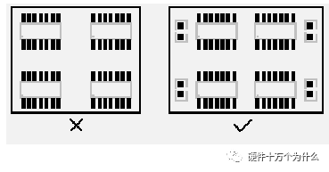
1. Follow the layout principle of "big first, then small, difficult first, easy first", that is, important unit circuits and core components should be laid out first. 2. The principle block diagram should be referred to in the layout, and the main components should be arranged according to the main signal flow of the board. 3. The arrangement of components should be convenient for debugging and maintenance, that is, large components cannot be placed around small components, components to be debugged, and there must be enough space around the components. 4. For the circuit parts of the same structure, use the "symmetrical" standard layout as much as possible; 5. Optimize the layout according to the standard of uniform distribution, balanced center of gravity, and beautiful layout; 6. The same type of plug-in components should face one in the X or Y direction Orientation placement. The same type of polarized discrete components should also strive to be consistent in the X or Y direction to facilitate production and inspection. 7. The heating elements should generally be evenly distributed to facilitate the heat dissipation of the veneer and the whole machine. Temperature sensitive devices other than the temperature detection element should be kept away from the components with a large amount of heat. 8. The layout should meet the following requirements as far as possible: the total connection is as short as possible, and the key signal line is the shortest; high voltage, high current signal and low current, low voltage weak signal are completely separated; analog signal and digital signal are separated; high frequency signal Separate from low-frequency signals; the spacing of high-frequency components should be sufficient. 9. The layout of the decoupling capacitor should be as close as possible to the power supply pin of the IC, and the loop formed between it and the power supply and ground should be the shortest. 10. In the component layout, appropriate consideration should be given to placing the devices using the same power supply together as much as possible to facilitate future power supply separation.
Two, wiring
(1) Wiring priority
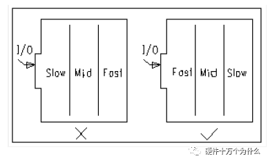
Key signal line priority: Prioritize routing of key signals such as small signals, high-speed signals, clock signals, and synchronization signals. Density priority principle: Start routing with the most complicated devices on the board. Start wiring from the most densely connected area on the board. Note: a. Try to provide dedicated wiring layers for key signals such as clock signals, high-frequency signals, and sensitive signals, and ensure the smallest loop area. When necessary, methods such as manual priority wiring, shielding and increasing safety distance should be adopted. Ensure signal quality. b. The EMC environment between the power layer and the ground layer is relatively poor, so avoid placing signals that are sensitive to interference. c. Networks with impedance control requirements should be routed according to the line length and width requirements.
(2) Four specific wiring methods
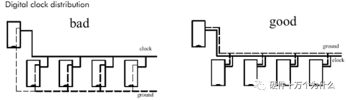
1. Clock wiring:
The clock line is one of the factors that have the greatest impact on EMC. Make fewer holes in the clock line, try to avoid running the line with other signal lines, and keep it away from general signal lines to avoid interference to signal lines. At the same time, avoid the power supply on the board to prevent the power supply and the clock from interfering with each other. If there is a dedicated clock generating chip on the board, no wires should be routed under it, and copper should be laid under it, and the ground can be specially cut if necessary. For crystal oscillators that many chips have reference, there should be no traces under these crystal oscillators, and copper isolation should be laid.
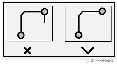
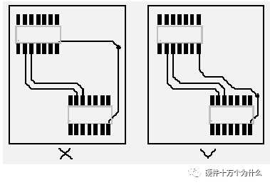
2. Right-angle routing:
Right-angle wiring is generally a situation that needs to be avoided as much as possible in PCB wiring, and it has almost become one of the standards for measuring the quality of wiring. So how much influence will the right-angle wiring have on signal transmission? In principle, right-angle routing will change the line width of the transmission line, causing discontinuity in impedance. In fact, not only right-angled wiring, but also corners and sharp-angled wiring may cause impedance changes. The influence of right-angle wiring on the signal is mainly reflected in three aspects: one is that the corner can be equivalent to a capacitive load on the transmission line, which slows down the rise time; the other is that impedance discontinuity will cause signal reflection; the third is that the right-angle tip is generated EMI.
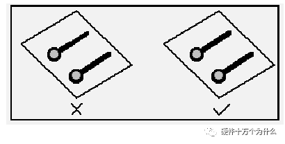
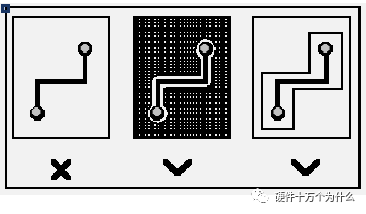
3.Differential routing:
See: Altium Designer - Differential routing and impedance matching
Differential signal (Differential Signal) is more and more widely used in high-speed circuit design. The most critical signal in the circuit is often designed with a differential structure. Definition: In layman's terms, the driver sends two equal and inverted Signal, the receiving end judges the logic state "0" or "1" by comparing the difference between the two voltages. The pair of traces carrying differential signals is called differential traces.
Compared with ordinary single-ended signal traces, differential signals have the most obvious advantages in the following three aspects: a. Strong anti-interference ability, because the coupling between two differential traces is very good, when there is noise interference from the outside world , Is coupled to two lines almost at the same time, and the receiving end is only concerned with the difference between the two signals, so the external common mode noise can be completely cancelled out. b. It can effectively suppress EMI. For the same reason, due to the opposite polarity of the two signals, the electromagnetic fields radiated by them can cancel each other out. The tighter the coupling, the less the electromagnetic energy leaked to the outside world.
c. The timing positioning is accurate. Because the switch change of the differential signal is located at the intersection of the two signals, unlike ordinary single-ended signals, which rely on the high and low threshold voltages to determine, it is less affected by the process and temperature, which can reduce the error in the timing. , But also more suitable for circuits with low amplitude signals. The current popular LVDS (low voltage differential signaling) refers to this small amplitude differential signaling technology.
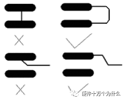
For PCB engineers, the most concern is how to ensure that these advantages of differential wiring can be fully utilized in actual wiring. Perhaps anyone who has been in contact with Layout will understand the general requirements of differential wiring, that is, "equal length and equal distance". The equal length is to ensure that the two differential signals maintain opposite polarities at all times and reduce the common mode component; the equal distance is mainly to ensure that the differential impedance of the two is consistent and reduce reflection. "As close as possible" is sometimes one of the requirements of differential wiring.
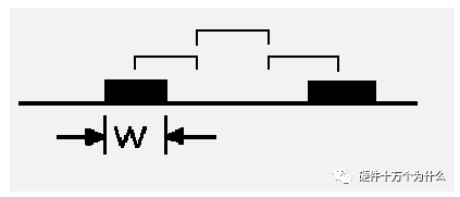
4. Serpentine line:
Snake line is a type of wiring method often used in Layout. Its main purpose is to adjust the delay to meet the system timing design requirements. The designer must first have this understanding: the serpentine line will destroy the signal quality, change the transmission delay, and avoid using it when wiring. However, in actual design, in order to ensure that the signal has sufficient hold time, or to reduce the time offset between the same group of signals, it is often necessary to deliberately wire.
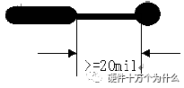
Note: The differential signal lines appearing in pairs are generally routed in parallel, with as few holes as possible. When holes are required, the two lines should be punched together to achieve impedance matching. A group of buses with the same attribute should be routed side by side as much as possible, and the length should be as equal as possible. The vias leading from the patch pad should be as far away as possible from the pad.
(3) Common rules for wiring
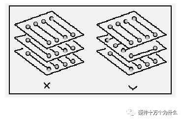
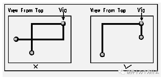
1. Direction control rules for routing:
That is, the routing directions of adjacent layers are orthogonal. Avoid running different signal lines in the same direction on adjacent layers to reduce unnecessary inter-layer interference; when it is difficult to avoid this situation due to board structure limitations (such as certain backplanes), especially when the signal rate is high, You should consider using a ground plane to isolate each wiring layer, and using a ground signal line to isolate each signal line.
2. Open loop inspection rules for wiring:
Generally, it is not allowed to have a floating line at one end (Dangling Line), mainly to avoid the "antenna effect" and reduce unnecessary interference radiation and acceptance, otherwise it may bring unpredictable results.
3. Impedance matching inspection rules:
The wiring width of the same network should be kept consistent. Variations in line width will cause uneven line characteristic impedance, and reflections will occur when the transmission speed is high. This situation should be avoided in the design. Under certain conditions, such as the lead wires of the connector and the similar structure of the lead wires of the BGA package, the change of the line width may not be avoided, and the effective length of the middle inconsistent part should be minimized.
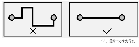
4. Wire length control rules:
That is to say, the short-circuit rule. When designing, you should try to keep the wiring length as short as possible to reduce interference problems caused by excessively long wiring. Especially for some important signal lines, such as clock lines, be sure to place their oscillators close to the device. The place. In the case of driving multiple devices, the network topology should be decided according to the specific situation.
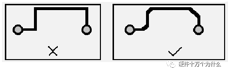
5. Chamfering rules:
In PCB design, sharp angles and right angles should be avoided to generate unnecessary radiation, and the process performance is not good.
6. Device decoupling rules:
A. Add necessary decoupling capacitors on the printed board to filter out interference signals on the power supply and stabilize the power signal. In multi-layer boards, the position of decoupling capacitors is generally not very demanding, but for double-layer boards, the layout of decoupling capacitors and the wiring method of the power supply will directly affect the stability of the entire system, and sometimes even the design. Success or failure. B. In the double-layer board design, the current should generally be filtered by the filter capacitor before being used by the device. C. In high-speed circuit design, whether decoupling capacitors can be used correctly is related to the stability of the entire board.
7. Partition/layering rules of device layout:
A. It is mainly to prevent mutual interference between modules of different operating frequencies, and to shorten the wiring length of the high-frequency part as much as possible. B. For hybrid circuits, there is also a way to arrange analog and digital circuits on both sides of the printed board, using different layers of wiring, and isolating the middle with a ground layer.
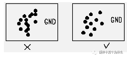
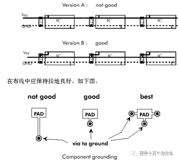
8. Ground circuit rules:
The minimum loop rule is that the loop area formed by the signal line and its loop should be as small as possible. The smaller the loop area, the less external radiation and the less interference from the outside world.
9. Integrity rules of power and ground plane:
For areas with dense vias, care should be taken to prevent holes from being connected to each other in the hollowed-out areas of the power supply and the ground layer, forming a division of the plane layer, thereby destroying the integrity of the plane layer and causing the signal line to increase the loop area of ​​the ground layer .
10. 3W rules:
In order to reduce crosstalk between lines, the line spacing should be large enough. When the line center spacing is not less than 3 times the line width, 70% of the electric field can be maintained without mutual interference, which is called the 3W rule. If you want to achieve 98% of the electric field without interfering with each other, you can use a spacing of 10W.
11. Shield protection
Corresponding to the ground loop rules, in fact, it is also to minimize the signal loop area, which is more common in some important signals, such as clock signals and synchronization signals; for some particularly important and high-frequency signals, copper cables should be considered Shielding structure design, that is, to isolate the left, right, and left lines of the wiring, and consider how to effectively combine the shielding ground with the actual ground plane.
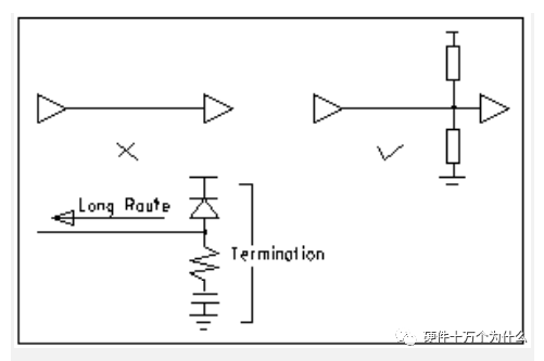
12. Wiring termination network rules:
In high-speed digital circuits, when the delay time of PCB wiring is greater than 1/4 of the signal rise time (or fall time), the wiring can be regarded as a transmission line. In order to ensure that the input and output impedance of the signal matches the impedance of the transmission line correctly, Various forms of matching methods can be used, and the selected matching method is related to the connection mode of the network and the topology of the wiring.
A. For point-to-point (one output corresponds to one input) connection, you can choose the start-end series matching or the terminal parallel matching. The former has a simple structure and low cost, but has a large delay. The latter has a good matching effect, but has a complicated structure and a high cost. B. For point-to-multipoint (one output corresponds to multiple outputs) connection, when the topology of the network is a daisy chain, terminal parallel matching should be selected. When the network is a star structure, you can refer to the point-to-point structure. Star and daisy chain are two basic topological structures. Other structures can be seen as a deformation of the basic structure, and some flexible measures can be taken to match. In actual operation, factors such as cost, power consumption, and performance should be taken into account. Generally, perfect matching is not pursued, and interference such as reflections caused by mismatches should be limited to an acceptable range.
13. Wiring closed loop inspection rules:
Prevent signal lines from forming self-loops between different layers. Such problems are prone to occur in multi-layer board design, and self-loop will cause radiation interference.
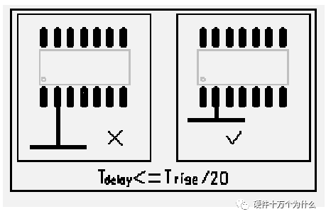
14. The branch length control rule of wiring:
Try to control the length of branches, the general requirement is Tdelay
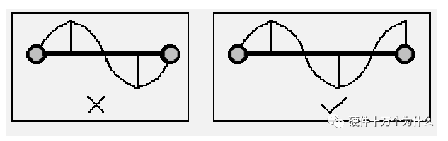
15. Resonance rules of wiring:
Mainly for the design of high-frequency signals, that is, the length of the wiring must not be an integer multiple of its wavelength to avoid resonance.
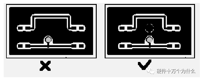
16. Isolated copper zone control rules:
The appearance of isolated copper areas will bring about some unpredictable problems. Therefore, connecting the isolated copper areas with other signals can help improve the signal quality. Usually, the isolated copper areas are grounded or deleted. In actual production, PCB manufacturers add some copper foil to the vacant parts of some boards. This is mainly to facilitate the processing of the printed board, and it also has a certain effect on preventing the warping of the printed board.
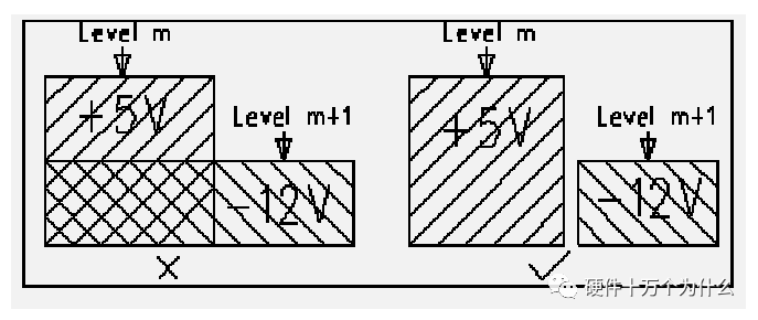
17. Overlapping power and ground layer rules:
Different power layers should avoid overlapping in space. The main purpose is to reduce the interference between different power supplies, especially between power supplies with very different voltages. The problem of power plane overlap must be avoided. If it is unavoidable, consider the intermediate ground.
18. 20H rule:
Since the electric field between the power layer and the ground layer is changing, electromagnetic interference will radiate outward from the edge of the board. It is called the edge effect. The solution is to shrink the power layer so that the electric field is only conducted within the ground layer. Taking a H (the thickness of the medium between the power supply and the ground) as a unit, if the shrinkage is 20H, 70% of the electric field can be confined to the edge of the ground layer; if the shrinkage is 100H, 98% of the electric field can be confined.

(4) Other
For single and double-layer boards, the power cord should be as thick and short as possible. The width requirements of the power line and the ground line can be calculated based on the 1mm line width corresponding to the maximum current of 1A, and the loop formed by the power supply and the ground should be as small as possible.
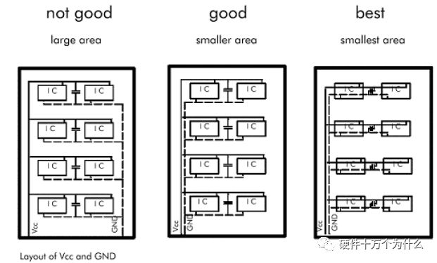
In order to prevent the coupling noise on the power line from directly entering the load device when the power line is long, the power supply should be decoupled before entering each device. And in order to prevent them from interfering with each other, the power supply of each load is independently decoupled and filtered before entering the load.
Zgar International (M) SDN BHD , https://www.sze-cigarette.com