A more convenient method is to use a three-terminal voltage regulator integrated circuit 7805 to form a step-down regulator circuit to obtain a 5V DC output.
The regulated power supply consisting of three-terminal regulator IC7805 has overvoltage protection, overcurrent protection and overheat protection. The performance is very stable and the output current is ≥1A. Only a small amount of peripheral components are required, and the circuit is simple and easy to manufacture. Typical diagram is as follows
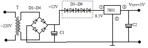
C1---Input filter capacitor, C2---output filter capacitor, 7805---regulator IC, D5~D9---buck diode.
D5~D9 will reduce the input voltage and reduce the power consumption of 7805. Usually the lowest input voltage of the 7805 regulator IC is 3-4V higher than the output voltage. The voltage difference between the output and the input directly leads to a large power loss. If calculated according to the output current 1A, there will be 1W power consumption per volt drop on the IC. Connecting 5 diodes in series to step down 3.5V can reduce the power consumption by about 3W, which is beneficial for the stable operation of the 7805.
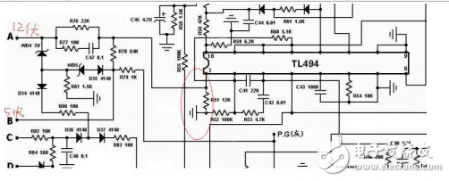
12 volts to 5 volts simple circuit diagram (2)
During the first 12V regulation process, R76, R77, C47 and R51 form a differential circuit, which does not work when 12V is stable. When the peak voltage C47 of 12V voltage appears to be short-circuited, the R76 suddenly R77 parallel equivalent structure is reduced, so that the voltage applied to the upper end of R51 will increase instantaneously to accelerate. 1L, v$D#y5r(S
During the second 5V regulation process, when there is no overvoltage or spike, it is assumed that 12V is stable, that is, the upper end of R78 is a stable voltage, and the 5V voltage is abrupt, which will cause the voltage across R78 to change. Assuming that the 5V voltage rises, then the voltage across R78 should be reduced, the resistance is a linear device, the organization is constant, and its voltage reduction directly causes its current to decrease. According to the power saving current method, 5V and The total current of the R78 series connection will also decrease (the shunt decreases), then the current flowing to R51 will increase, causing the voltage of R51 to be added to achieve voltage regulation and adjustment. %_/](VU-k&V
In addition, in order not to make the circuit too sensitive to the sudden spike of the power grid, the two points of AB are separately analyzed for AC grounding, and the hidden integration circuit can be analyzed, but it is not very useful for maintenance.
The SCC3 service operates from the current solar panel input through the third quarter and IC3 power control circuits. When the voltage of the solar panel exceeds 12V, the Zener diode ZD1 acts to open the third quarter and provides the power IC3. The production of IC3 is regulated by a 5 volt power supply. Use the logic of the 5V power supply circuit and compare it as a reference voltage to the battery float voltage.
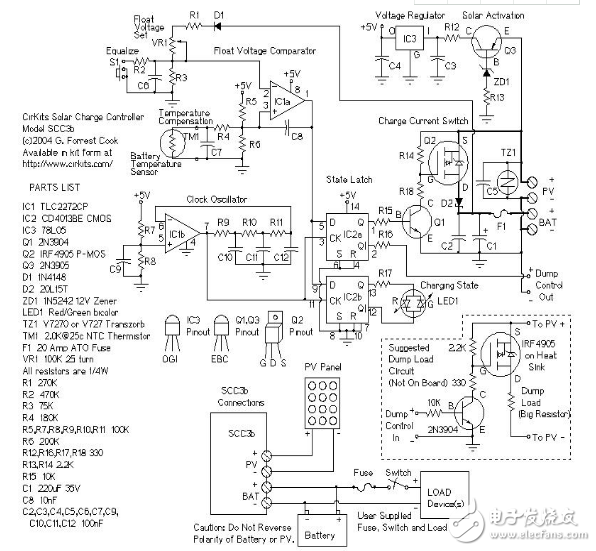
The floating voltage comparator IC1A compares the reference voltage (divided by R5 and R6) the battery voltage (divided by R1/VR1 and R3). The comparison point is offset by the thermistor temperature compensated TM1. The comparison points of the peer switches S1 and R2 are also modified. The output of IC1a is high (+5V) when the battery voltage is lower than the float voltage setting. The output goes low when the battery voltage is higher than the float voltage setting. This provides a charge/idle signal that controls the rest of the circuit.
The charge/idle signal is sent to IC2A and B, a pair of D-type flip-flops. The flip-flop clock IC1B phase shift clock oscillator. The clock causes the output of the flip-flop to generate a square wave charge/idle signal that synchronizes the frequency of the clock oscillator. The two halves of IC2BIC2 operate synchronously. IC2A is used to drive the current switching circuit to drive the charge status indicator LED red (charge) or green (floating).
The clock's charge/idle signal switches the bipolar transistor Q1 and turns off. The Q1 signal is used to switch the power MOSFET Q2, switch the current of the solar cell, and pass it off. The solar charging current flows through the thick line on the schematic. Diode D2 prevents batteries that are discharged through the solar panel during the night. Fuse F1 prevents flow in the battery over current short circuit event. TranszorbTZ1 absorbs transient voltage spikes that may be caused by lightning.
Shenzhen Kaixuanye Technology Co., Ltd. , https://www.icoilne.com