Functional testing is becoming more and more important, but as with online testing, technology development and PCB design can limit the scope of testing. Although much progress has been made in programming the software environment to help overcome some of these difficulties, there are still many issues to avoid and to be more prepared if you want to successfully implement functional testing in accordance with your testing strategy. This article describes some of the factors and coping strategies that should be considered to successfully implement functional testing.
Electronic product functional testing has a history of its rise and fall. In the late 1960s, it was the first automated test method. With the advent of online test technology in the late 1970s, functional testing seemed destined to give way to easier and faster online testing of programming and judgment. . However, today, the trend has changed. There is a problem with online testing that is getting more and more serious, that is, the detection method. According to the analysis of the US NEMI (National Electronics Manufacturing Organization), the nodes that can be detected by the end of 2003 will basically be zero. If the detection is impossible, the online test will almost no use.
Functional testing is increasingly being used in post-production processes and even in mid-process testing, but its systems and implementation methods are almost completely different from previous tests. Today's test systems are faster and more compact in most cases, and functional tests verify the overall functionality of the product, maintain calibration information, provide data to ISO9000 programs, and ensure the quality of high-risk products such as medical equipment. Indispensable.
The method of implementation of the test is influenced by factors such as budget, production, and design of the product to be tested (UUT), and it is the last item that can measure the most impact, and the budget and output will limit the test. In order to get the highest possible fault coverage for the test, you must pay attention to the component selection and PCB layout during the design phase. Unfortunately, the actual situation is not always the case. The rush to enter the market and the intense development will often upset you. Wishful abacus.
Here is a preliminary analysis of how to deal with these restrictions. Some concessions that have to be made for testing (especially in the early stages of design) can affect the design, but make testing easier and improve test failure coverage. Please note that the following questions and suggestions are not faced or need to be addressed by every test engineer. Many of these issues will affect each other, so each issue should be evaluated and applied flexibly when needed.
What are the test requirements for the product to be tested?
Before discussing design, test systems, software, and test methods, you need to understand the "object" - the product to be tested, not only the PCB or the final assembly itself, but also the amount of production, the expected failure, etc. Including: product category
Structure (single PCB / pre-made PCB / final product)
Test specification plan test point expected output (per line / day / shift, etc.)
Expected fault type
Obviously, the "budget" is ignored above, but only after understanding the above items can we determine how much it costs to test a product. After we have figured out what it takes to fully test the UUT, we can start discussing the funding problem. Only at this time can we only Know how to make a compromise to get the job done. After the initial report is completed, the company may give you a budget and wish you "good luck" - figuring out what you can do, you really need "good luck" at this time, but there are other things, listed below some.
High-density problems On the surface, component density is not a problem for functional testing. After all, the main consideration here is to "get the correct output for one input." It is true that it is a bit too simple, but the actual situation is like this. Applying a given excitation signal to the UUT input, the UUT will output a specific series of data after a certain time, and the connection to the I/O connector should be the only access problem.
However, the density of components also has a certain impact. Looking at the PCB sample of Figure 1 (or your own design), you must first answer the following questions; need to access the calibration circuit?
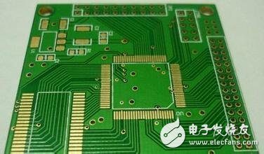
Figure 1 PCB sample
Is it important to diagnose a UUT specific component or a specific area?
If there is a positive opinion on the answer to the above question, is the investigation done by people or by some kind of automatic mechanical device?
Do you want to use an automated test set?
Is the I/O connector used easy to touch or connect? If not, is the connector a through-hole mount that can be accessed through the needle bed?
Let's discuss these issues one by one.
Calibration circuit function tests are often used for calibration or verification of analog circuits, including checking the internals of the UUT (such as the IF portion of the RF circuit) to verify its operation, which may require test points or test pads. One problem with high frequency design is that the relative impedance of the test point (path length, test pad size, etc.) plus the impedance of the probe can affect the performance of the circuit. Keep this in mind when setting up the test area, and automated mechanical detection. And the needle bed clamp (discussed later in this article) requires only a small test area to alleviate this contradiction, mainly because the accuracy of the robot itself allows the tester to detect smaller areas than manual operation. .
Troubleshooting If you only want to use the functional test as a pass/fail filter without measuring the calibration point, you can skip this section because the application may not require a probe at this time. In most cases, the functional test passes the pass/fail test because the functional test is very slow in diagnosing the fault, especially in the event of multiple faults. But in some industries, functional testing is moving into manufacturing processes, such as cellular phone manufacturing, where some manufacturers make certain critical measurements at the PCB level, that is, during assembly before final assembly, which is done by The nature of the phone is easily eliminated. In other words, mobile phones are designed to be assembled at a lower cost, they are not easy to disassemble, so verifying the function before final measurement can save rework costs and reduce possible waste (because the phone will be damaged when it is unpacked).
Therefore, it is necessary to have sufficient test points to probe the PCB. For example, it is not convenient to check the J-lead of a 20 mil surface mount device, and the BGA is even less likely. According to the recommendations of the American Surface Mount Technology Association (SMTA), the test point spacing is a minimum of 0.040 inches. The spacing between the pads depends on the component height around the test area, the probe size, etc., but the 0.200 inch spacing should be the minimum requirement. Especially the artificial exploration area. Obviously, test fixtures and robotic probes are more accurate.
Test design is undoubtedly a design that is easy to test is easier to handle in production than a casual design. But engineers often want to load more technology at the lowest cost in the smallest volume, an idea that increases the limits of contact with the board during online and functional testing.
There has also been a reaction to this type of problem market, and software tools are now available to analyze designs, review them according to the rules laid down in assembly and test equipment, and suggest ways to make PCBs easier to produce. If these tools are suitable for your product, it is recommended to analyze each design, at least it can quickly point out where the test contact is found, and the ultimate goal is to make the product easier to manufacture.
Structural configuration that meets high density requirements
The high density can be either a small PCB size, a large number of circuits on the UUT, or both. The above description indicates that the mechanical and electrical structure of the system must be considered to meet the test requirements. The mechanical issues to consider are:
How to support UUT test area multi-layer board test (can the tester do parallel test?)
I/O connector
In terms of electrical, if it is a multi-layer board, which one is more economical? Is it a multi-instrument or a switching converter with a small number of instruments? Depending on the UUT structure or the type of instrument required, the answer may not be easy to come by.
Auto or manual?
As the production and speed of each line increase (a major way to achieve economies of scale is to increase the productivity of each test equipment), consideration should be given to whether the test process can be automated. Automated functional testing virtually eliminates the need to load/unload and eliminates the need to add additional test systems, often without regard to the increased cost of transport equipment when considering increased throughput.
Disadvantages of test automation include an initial hardware investment, time to integrate with the production line, whether the test system can be synchronized with the line speed, and problems with production if the device fails. The off-line tester does not directly affect the assembly line. If the tester fails, the product can be taken out of the production line and the production line will continue to be produced, so that the production line will not be affected, but processing time and labor are also a problem.
It should be borne in mind that manual testing usually involves the use of several cables and connectors to connect the UUTs. These cables are generally less durable than the probes on the needle bed fixtures and should be included in the maintenance plan, which reduces the A malfunction.
Shenzhen Guan Chen Electronics Co., Ltd. is a High-tech enterprise that integrates R&D, design, manufacture of computer peripheral products.The products include Thunderbolt Docking Station,USB Docking Station,USB Hubs,USB Adapter, Thunderbolt Cable, SSD Enclosure , HDD Enclosure . Our company adheres to the principle and motto of Being sincere, Responsible, Practical to meet the needs of markets and customers with high quality technology and management. We commit ourselves to new product development and also stress the exploring of international markets.
Our company owns a professional production team and establishes strict quality control standard, so we can provide high quality products and service for customers. We have Grapgic designer,3D Deisnger and Electronic designer to provides professional OEM/ODM service. Our factory covers an area of 1,000-2000 spare meters, which houses 100-200 workers, so our production capacity reaches 50,000 pieces every day.With more than 10 engineers focusing on research and development, our private model attracts much among different markets. Over 100 new designed models are released per year.There are also 3 lean production lines to fullfill small quatity orders production for variety of models.
Our Thunderbolt 3 Docking Station has passed thunderbolt certified by intel and apple.Our product also all can meet with CE, RoHS, UL, FCC and other related certification.And our factory also meets legal environmental standards ensuring your order is delivered. We have a very good reputation at home and abroad. Our products are mainly exported to Europe, USA and Southeast Asia. We provide one-stop-service and promote customers achieve rapidly development. Customer comes First, Quality Ranks First, and Reasonable Price.Guanchen will be your faithful partner from China.
Type C To Network Adapters,Type-C To Network Hubs Rj45 Adapter,Network Hubs Rj45 Adapter,Usb-C To Gigabit Network Adapter
Shenzhen GuanChen Electronics Co., Ltd. , https://www.gcneotech.com