Circuit function and advantage
Whether the IQ modulator is used for direct conversion applications or as an upconverter for the first intermediate frequency (IF), there is usually some gain directly applied after the IQ modulator. This article describes how to select the appropriate driver amplifier to provide the first stage gain at the output of the IQ modulator. The device shown in Figure 1 is the ADL5375 IQ modulator and the ADL5320 driver amplifier. Both devices are well matched at the system level; that is, they have the same performance, so neither side will cause overall performance degradation. Because of the good dynamic range matching of these devices, it is recommended to make a simple direct connection between the IQ modulator and the RF driver amplifier without any attenuation between the devices.
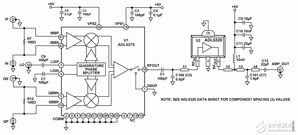
Figure 1. Schematic diagram of an IQ modulator circuit with output power gain
Circuit description
The ADL5375 is a general purpose, high performance IQ modulator with an output frequency range of 400 MHz to 6 GHz. With low noise and a wide input baseband bandwidth of 750 MHz (3 dB), the device can be driven with multiple modulation and bandwidth signals. These input signals can be centered on either a DC or a complex intermediate frequency.
The LO interface with the ADL5375 is 1XLO type, that is, the output frequency and the LO frequency are equal (when the baseband signal is centered on DC).
System level calculation and RF amplifier selection
In the frequency range of 1 GHz to 2 GHz, the output compression point (OP1dB) and third-order compression point (OIP3) of the ADL5375 are around 10 dBm and 25 dBm, respectively. When selecting an RF amplifier to provide gain after the IQ modulator, the device with input P1dB and input IP3 equal to or slightly above these values ​​must be selected. If the input P1dB and input IP3 of the selected device are lower, the cascading performance will be degraded; if these two specifications are significantly higher than the ADL5375, it will not bring any benefits and may cause the total supply current of the signal chain to appear. No need to increase.
The ADL5320 is a driver amplifier (an RF amplifier that requires an external tuning component) and is rated for operation from 400 MHz to 2700 MHz. With a 5 V supply, it consumes 104 mA (it can also be powered from a supply as low as 3.3 V, where power and performance are degraded).
Table 1 shows the specifications for the IP3 (OIP3) and P1dB (OP1dB) of the ADL5375 IQ modulator to the output at 1900 MHz and the ADL5320 driver amplifier to the input. In both cases, the specification of the IQ modulator to the output differs from the specification of the amplifier to the input by about 3 dB.
Table 1. IP3 and P1dB Specifications for ADL5375 IQ Modulators and ADL5320 Driver Amplifiers at 1900 MHz
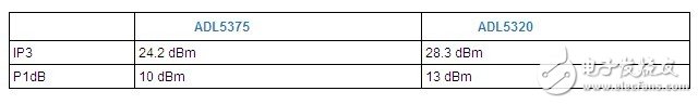
Figure 2 shows the simulated cascade performance of the IQ modulator and driver amplifier at 2140 MHz. This simulation is done using the ADIsimRF design tool. It is worth noting that the difference between the modulator's OIP3 (24.2 dBm) and the composite OIP3 (36.5 dBm) is just slightly less than the gain of the ADL5320 driver amplifier (13.7 dB). This indicates that the driver amplifier has a very small effect on the overall OIP3.
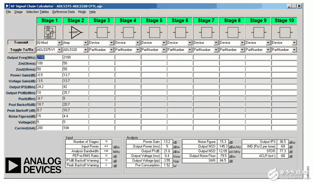
Figure 2. Screen capture of the ADIsimRF design tool showing the cascading performance of the ADL5375 and ADL5320
Figure 3 shows the relationship between OIP3 and output power (POUT) measured at the output of the IQ modulator and the output of the composite circuit. The shape of the two OIP3 curve profiles is very similar, with only an offset in output power and OIP3. This further shows that IP3 will only drop slightly when the signal passes through the RF amplifier.
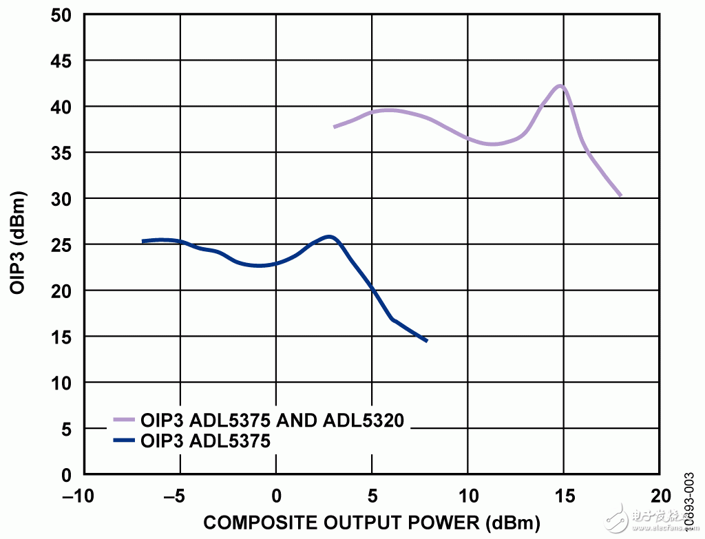
Figure 3. Relationship between OIP3 and POUT of the ADL5375 IQ modulator and composite circuit (ADL5375 and ADL5320 driver amplifiers) at 2100 MHz
USB4 specifies tunneling of:
USB 3.2 ("Enhanced Superspeed") Tunneling
DisplayPort 1.4a -based Tunneling
PCI Express (PCIe)-based Tunneling
Main Benefits of USB 4
The new USB 4 standard has three main benefits over prior versions of USB.
40 Gbps Maximum Speed: By using two-lane cables, devices are able to operate at up to 40 Gbps, the same speed as Thunderbolt 3. The data is transmitted in two sets of four bidirectional lanes.
DisplayPort Alt Mode 2.0: USB 4 supports DisplayPort 2.0 over its alternative mode. DisplayPort 2.0 can support 8K resolution at 60 Hz with HDR10 color. DisplayPort 2.0 can use up to 80 Gbps, which is double the amount available to USB data, because it sends all the data in one direction (to the monitor) and can thus use all eight data lanes at once.
Better Resource Allocation for Video, PCIe: In lieu of alternative mode where the other interface takes over the connection, USB 4 devices can use a process called "protocol tunneling" that sends DisplayPort, PCIe and USB packets at the same time while allocating bandwidth accordingly.
Usb4 Cable,Usb To Usb4,Usb 4 Cable,Usb 4 Wires
UCOAX , https://www.ucoax.com