introduction
Today's power market, fight volume, price, performance, how to do these 3 points requires an experienced layout engineer.
1, static damage IC1. The closer the VCC capacitor is to the VCC pin, the better. As shown in the figure below, the VCC capacitor is too far away from the IC pin. Static electricity and withstand voltage will damage the IC. Of course, this depends on the chip's anti-ESD capability.
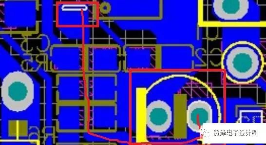
2, single point grounding, static and pressure-resistant circuit is the same , first we figured out that its circuit is basically clear, the main two parts, Y capacitor, transformer primary and secondary parasitic capacitance. Therefore, the ground of these two devices should be grounded at a single point as far as possible to prevent damage to the IC.
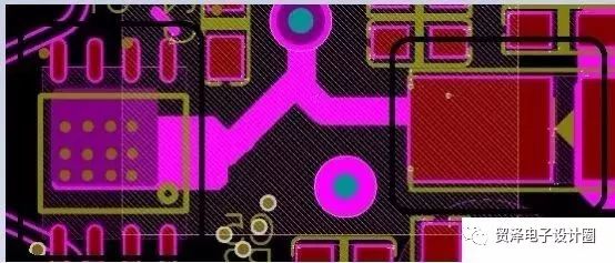
3, the following is the most depressed, 10KV air is okay, 15KV hangs, direct bombing, and finally transferred to fear. Later, the curtains were turned off in the red part of the figure below. A cheerful little spark of the Y capacitor turned to the MOS, which means that the 15KV was farther away. Later, the slot was pulled and a part of the insulating sheet was isolated.
4, the discharge needle, do not underestimate a small discharge needle, the key time is a big effect, I have actually seen, as shown in the following figure in a dark room, playing 15KV static electricity, both ends of the discharge arc to produce a spark consumption Drop it. Pay attention to the safety distance.
A board of experienced engineers and a relatively amateur to make a temperature difference of 10-20 degrees, you believe, I believe.
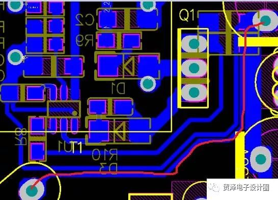
1, Schottky temperature is high, so change the package and current to change the brand than the brand, in fact, Layout can also be solved, the Schottky anode is connected to the mother seat, the temperature of the Schottky can be lowered by 10 degrees. effect.
2, then the above figure, Schottky temperature down, the mother seat has improved, the transformer and MOS are too close to the mother seat, can also be understood as the distance between the power devices is too close, we know the transformer MOS Schottky These power devices, the worse the performance in the worsening environment, result in higher temperatures. As shown in Figure 2 below, the IC temperature of Schottky and the built-in MOS differs by 7 degrees.
3, using all available heat, often hear an IC, FAE said that our IC temperature is 100 degrees to actually make 120 degrees, which is to see the drawing board. Car charger, open the window, thicken the copper foil, use the negative elastic to export the heat. Originally 125 degrees, the above 3 points are added to reduce 20 degrees. You believe that I believe. Q2 synchronous rectification, open the window directly to the negative shrapnel, Q1 switch tube, U1IC principle Q1Q2. Synchronize 2OZ.
The 130 degree chart is also on the top. This board Q1 125 degrees Q2 134 degrees IC 120 degree inductance 120 degrees.
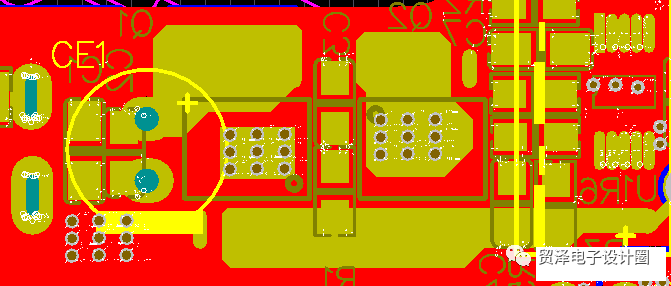
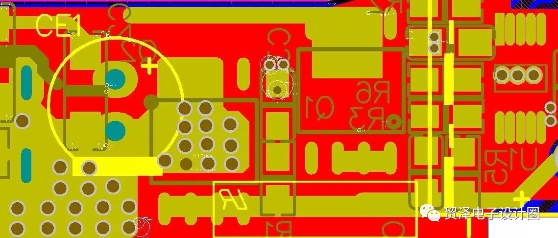
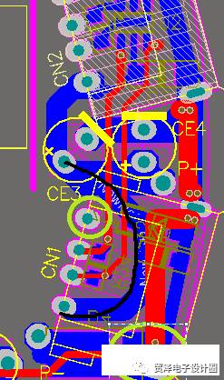
Ripple Everyone knows that this affects the ESR of the capacitor, increases the capacity, and adds the differential mode inductor to reduce the ripple current to form a π filter. As mentioned above, to reduce costs, the method is always more than the problem, first check the board. First look at the board below, CN1 ripple 90mV, CN2 ripple 150mV. Look carefully at the blue line below to outline the area of ​​the loop is too large, put CE3 in the middle of the two USB, the ripple is reduced to 100mV, if there is any difficulty, you can add a small capacitor on the CN2 end.
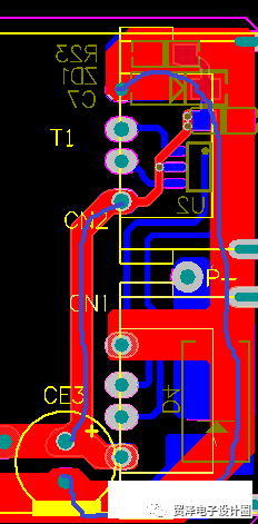
Do not go over the shortcuts in order, look at the figure below, the direction of the current is directly ignored by the ground of the capacitor, the ripple is nearly 300mV, we try to connect the ground of the transformer to C4 ground. Look at the current path to a complete loop, the ripple dropped to 73mV.
Also pay attention when you must add π filtering. The capacitance in front of the differential mode inductor should be greater than or equal to the capacity, otherwise it will easily cause oscillation.

The rectified Schottky should be close to the filter capacitor or it will be easy to oscillate. There is a serious high-pressure bomber. It is the following picture that once blew my heart.

EMI Daily debugging is nothing more than absorption, common mode, X capacitor, transformer shielding. In fact, the drawing board can also solve many problems.
1. MOS is too close to the transformer. Conducting NG, which is easy to distinguish, the average peak in many places is also super-peak. The distance between MOS and LN is basically solved.
2. The transformer and LN are too close. Similarly, NG is transmitted, and the peak-to-peak average is super-excellent in many places, often based on the drawbacks of the structure. Yes, the transformer plus shielding can be solved, you can try to put the transformer feedback and the secondary reverse winding. It is generally saved by solving this cost.
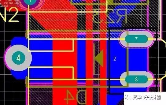
3. The junction of the Y capacitor. As shown in the following figure, the ground of the Y capacitor is directly connected to the ground of the large capacitor or the ground of the transformer. The output is low or positive. There is no hard index to see the actual effect. In many cases, it is still very obvious. Let's talk about the Y capacitor. It is better to add a charger to reduce the ripple noise and reduce the interference of the mobile phone. The adapter will look at the situation. For example, if the set-top box is added, there will be interference.
4, the car charger is more obvious is that the effect of the anode connection input point of the freewheeling diode is still very obvious.
Do not use the mother seat as the trace, the impedance greatly affects the efficiency, and has been tested to affect 0.5 points.
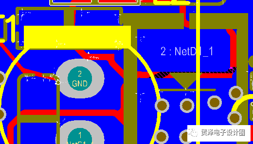
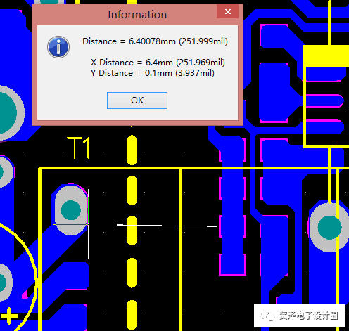
At an altitude of 5000m, we are currently certified to CCC to meet this requirement. The main difference is air creep, and the primary and secondary must meet 6.4mm.
The distance between the line and the half is greater than 0.8mm. Let us see a picture, almost pasted, and the actual material is only 0.4, which causes insufficient overcurrent capability.

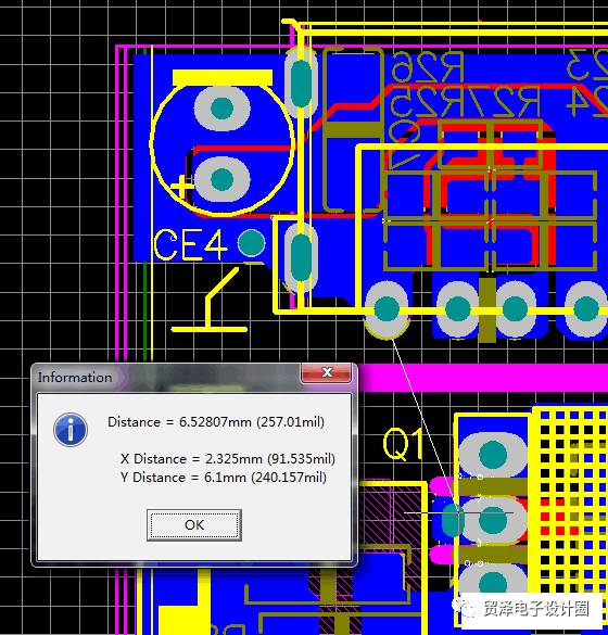
The shortest distance is about 8.5. At that time, the insulating sheet only included MOS and G poles.
12 Pin Automotive Connector Housing
Wenzhou Langrun Electric Co.,Ltd , https://www.langrunele.com