The future system development trend is to implement a programmable system-on-chip (SOPC), which integrates the CPU and interface circuits into a single chip. We use the EP1C6Q240C8 FPGA of Altera's Cyclone series devices, which can be embedded with Nios II soft core. By using the VHDL language to design the fingerprint reading interface UART plus the IP core required by the module, use the SOPC Builder in the Quartus II software to The Nios II system is built inside the FPGA, and then connected to the peripheral circuit through the pin configuration, and the peripheral device programming and fingerprint recognition algorithm design are realized in the Nios II IDE environment. Build a SOPC system with Nios II as the processing core, making the system more compact and flexible. At the same time, the front-end design of the fingerprint chip is also realized, which is also one of the research purposes of this subject, and then a very large-scale integrated circuit-fingerprint recognition chip is made through ASIC integrated design circuit technology. This expands the scope of application of fingerprint technology and application market areas, such as fingerprint car locks, fingerprint firearms, fingerprint handheld computers, mobile phones and other embedded applications.
Overall hardware design of the moduleThe hardware design of fingerprint recognition module adopts SOPC design idea [1], realize fingerprint reading UART interface, FLASH memory interface, SDRAM controller, PIO control keyboard and LCD display interface in FPGA. This makes full use of the IP core advantages of FPGA and uses SOPCBuilder to integrate these interfaces, controllers and PIOs into the FPGA. The various parts are connected through the Avalon bus to form a SOPC system with Nios II processor as the core, and then configure the pins through the TCL script language, and configure the input and output signals inside the FPGA to the IO pins of the FPGA to achieve the Peripheral devices fingerprint sensor, SDRAM memory chip, FLASH memory chip, keyboard and LCD display connection. Use the Nios II processor inside the FPGA for control to ensure that the module functions can be realized. The hardware block diagram of the whole recognition module is shown in Figure 1.
The function of each device of the entire module is: the function of the FLASH dedicated configuration chip is to store the program, and configure the program for the entire system every time it is powered on. Because FPGA is based on RAM structure, the program will be lost every time the power is off. The fingerprint reading interface UART is to connect the fingerprint sensor to read the fingerprint image correctly. The FLASH memory is used to store the fingerprint template data to ensure that the data is not lost after the fingerprint template is powered off. SDRAM memory is the random storage of input fingerprint data and the storage of fingerprint template data that is being matched. PIO control is to directly control the keyboard and LCD display with FPGA pins. There is a 4×4 button in the module, which has functions: input fingerprint key, delete fingerprint key, confirm key, reset key, delete input character key, shut down key, 0-9 character key. The LCD displays the matching result and the completion of each function. The central control and processing unit NiosII processor is mainly responsible for the coordination of the entire system, the operation of peripheral devices and the processing of fingerprint algorithms.
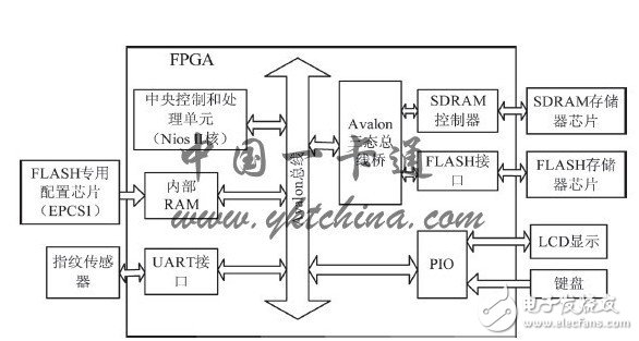
figure 1
Altera's Cyclone EP1C6Q240C8 FPGA, its LE number is 5980, there are 2 PLLs inside, and 3 types of Nios II processors can be embedded. And compared with other FPGAs, it can meet the module function and the price is relatively low. Therefore, this chip was selected in the design.
Use SOPC Builder to build Nios II hardware systemUse the SOPC Builder component to add the standard Nios II processor and RAM memory (onchip_memory) necessary for the normal operation of the entire system. This is the core processing unit of the entire fingerprint recognition module. The standard NiosII processor occupies FPGA1200LE resources, achieving a balance between performance and area, and can also meet the design requirements of this system in terms of performance, and is also ready for adding or modifying functions in the future. The selected data width of RAM memory is 32bits and the storage capacity is 4K byte. Used to store data in the program and data cache.
In order to communicate between the Nios II soft core and the external memory, an Avalon tri-state bus bridge must be added between the Avalon bus and the bus connecting the external memory [2]. It can be added directly from the Add SOPC Builder component menu, as shown in Figure 2:
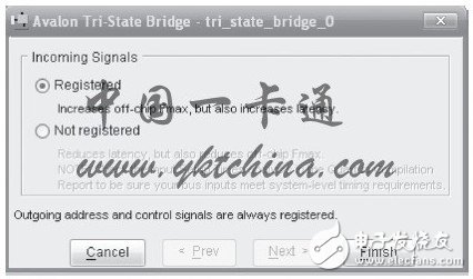
Figure 2 Analon three-state bus bridge
The biggest advantage of using SOPC Builder is the use of abundant IP core resources. Add SDRAM controller IP core, FLASH memory interface IP core, P IOIP core in SOPC Builder graphical interface. The SDRAM controller data bus uses 16 bits, the Banks select 4, the FLASH memory interface uses the address bus 20, the data bus is 16, the button selects 16 PIOs, the LCD control port selects 3 PIOs, and the data port selects 8 PIOs. The choice of data depends on the selected peripheral device. The use of IP core not only saves development time but also increases the stability of the system.
SOPC Builder has custom logic functions. The designed fingerprint reading interface UART, through the component compiler, create a UART component [3], find the UART in User Logic under Avalon Components, and add this UART component to the SOPC system. The Nios II processor, memory, and various interfaces added in SOPC Builder are connected together through the Avalon bus, and the modules are coordinated to work with each other under the coordination of the Nios II processor. The Avalon bus provides a channel that allows data to flow at high speed between modules. The problem of bus competition can be effectively solved with the help of the master-slave peripheral access mode supported by the Avalon bus. In this design, the data flow in the channel is divided into two response modes, active and passive. In the active response mode, the flow of data is actively proposed by each component, and in the passive response mode, each component can only respond to requests from other components. SOPC Builder allows the system to automatically assign base addresses through Auto-Assign Base Addresses. Let the system automatically assign interrupts through Auto-Assign IRQs. The overall hardware configuration diagram of the fingerprint recognition module is shown in Figure 3.
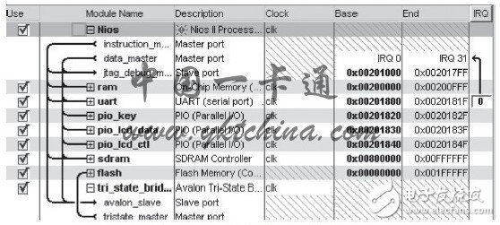
Figure 3 The overall hardware configuration diagram of the fingerprint recognition module
After configuring the hardware in SOPC Builder, run Generate to generate the Nios II system. The PLL system clock circuit inside the designed FPGA. When processing the fingerprint algorithm, use the function of the PLL (Phase Locked Loop) inside the FPGA to speed up the processing. In order to increase the storage speed of SDRAM memory, it is also necessary to increase the system clock. Use the megafunction module in Quartus II to design the PLL internal interface as shown in Figure 4, clk is the input clock of the PLL 25MHz. Ratio is the frequency multiplication/division coefficient, C0 is the clock input of Nios II, the frequency multiplication factor is 2, so the clock input of Nios II is 50MHz, C1 is the SDRAM clock input, the multiplication factor is 4, so the clock input frequency of SDRAM It is 100MHz.
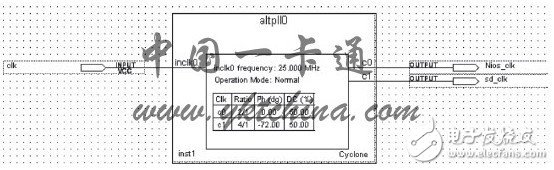
Figure 4 PLL internal interface designed with macro module
The Nios II system inside the FPGA after the entire SOPC design is shown in Figure 5. The TCL script is used to assign pins to the FPGA. The following is a section of SDRAM TCL script [4] program. Realize the connection with external devices.

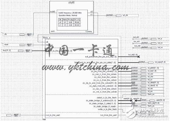
Figure 5 Nios II system diagram inside FPGA
in conclusionUsing the SOPC solution based on the Nios II processor can greatly shorten the development time and expand the flexibility of system development. SOPC has become a reality. With the continuous improvement of the performance of the Nios II core embedded processor and the continuous improvement of its development tools and IP core library, its use will be more extensive. I believe that in the near future, electronic product design engineers will be able to fully appreciate the convenience brought to their design by the Nios II processor system. It also provides a way for us to independently develop fingerprint recognition chips.
Heating Element Temperature Control,Electric Grill Temperature Controller,Thermostat For Heating Element,Oven Capillary Thermostat
Foshan City Jiulong Machine Co., Ltd , https://www.jlthermostat.com