Flash physical structure
Flash memory device principle
The previous article has talked about the development history of solid-state drives. In the past, solid-state drives used RAM and other media, but most of the current solid-state drives use flash memory chips as storage media. We rarely see DRAM solid-state drives, and they are mainly used in special occasions. The world's first solid-state drive, which was born in 1978, was based on DRAM. However, due to the power-down volatility of DRAM, and of course cost factors, current solid-state drives generally do not use DRAM, but use flash memory as a storage medium, which is NAND flash memory. Many of the working principles of SSDs are also based on the characteristics of flash memory. For example, flash memory must be erased before writing, and cannot be overwritten, so solid-state drives need garbage collection (garbage collection, or Recycle); the number of times of erasing and writing each block of flash memory reaches a certain value, and this block will either become Bad blocks, or the data stored on them is unreliable, so the SSD firmware must do wear leveling, so that the data is written evenly on all blocks, rather than staring at a few blocks and writing desperately (otherwise, the SSD will be scrapped soon). There are many similar examples. Many algorithms inside SSDs are serving flash memory. Therefore, if you want to attack solid-state drives, flash memory bears the brunt.
Flash memory is a type of non-volatile memory, which means that data will not be lost if power is lost. The basic storage unit of flash memory (Cell) is a kind of NMOS-like double-layer floating gate MOS transistor, as shown in Figure 3-1:
Figure 3-1 Floating gate transistor structure
A floating gate for storing electrons is formed on the semiconductor where the current is unidirectionally conducted between the source (Source) and the drain (Drain). The floating gate is surrounded by an insulating layer up and down, and the electrons stored in it will not disappear due to power failure. So flash memory is non-volatile memory.
The write operation is to apply a positive voltage to the control electrode, so that electrons enter the floating gate through the insulating layer. The erase operation is just the opposite. A positive voltage is applied to the substrate to suck out the electrons from the floating gate, as shown in Figure 3-2:
Figure 3-2 Left: Write principle; Right: Erase principle
At the Flash Memory Summit 2014, Dr. Simon Sze, the inventor of the floating-gate transistor, was awarded the Lifetime Achievement Award for his invention of the floating-gate transistor. It is said that the inspiration for the invention of the floating gate transistor came like this: One day, Shi Min and his partner Dawon Kahng had lunch together in the company cafeteria, and dessert was cheesecake. Looking at the layer cake, they were thinking, what would happen if you put something in the middle of the MOS FET? Thus, the floating gate transistor was born. As of some point in 2014, according to statistics, the number of floating gate transistors produced worldwide reached 1 074 344 929 692 350 000 000
This number continues to grow. Dummy felt that the Lifetime Achievement Award was not enough. Shi Min should have won the Nobel Prize. After all, the discoverer of the mechanism of mechanical hard disks, the giant magnetoresistance effect, has already won the Nobel Prize.
After winning the award, Shi Min ordered a cheesecake for herself at the celebration banquet.
SLC, MLC, TLC
A flash memory that stores 1-bit data is called SLC (Single Level Cell), 2-bit is MLC (Multiple Level Cell), and 3-bit is TLC (Triple Level Cell). There are already manufacturers developing QLC, that is, a memory cell stores 4-bit data, which is not introduced in this book.
Figure 3-3 SLC, MLC, TLC principle
For SLC, a memory cell stores two states. When there are more electrons in the floating gate than a certain reference value, we sample it as 0, otherwise, it is judged as 1.
Figure 3-4 shows the threshold voltage distribution function of the memory cells in the flash memory chip. The horizontal axis is the threshold voltage, and the vertical axis is the number of memory cells. In fact, at 0 or 1, not all memory cells have the same threshold voltage, but a distribution centered on this voltage. When reading the sampled voltage value, if it falls in the range of 1, it is considered to be 1; if it falls in the range of 0, it is considered to be 0.
After erasing, the value read from the flash memory is 1, and after charging, it is 0. Therefore, if you need to write 1, you don't need to do anything, and if you write 0, you need to charge to 0.

Figure 1-4 SLC voltage distribution (Source: Inside NAND Flash Memory)
For MLC, if a memory cell stores 4 states, it can only store 2 bits of data. Generally speaking, it is to divide the number of electrons in the floating gate. For example, if it is less than 10 electrons, it is judged as 0; if it is 11-20 electrons, it is judged as 1; if it is 21-30, it is judged as 2; if it is more than 30 electrons, it is judged as 1 Electronic, judged as 3.
Figure 1-5 MLC voltage distribution (Source: Inside NAND Flash Memory)
By analogy with TLC, if a memory cell has 8 states, then it can store 3 bits of data, which further divides the number of electrons in the floating gate on the basis of MLC.
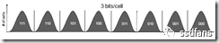
Figure 1-6 TLC voltage distribution (Source: Inside NAND Flash Memory)
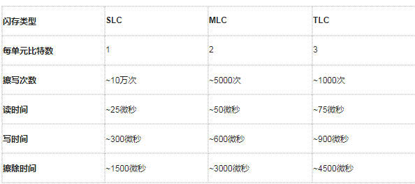
A memory cell of the same area, SLC, MLC and TLC, can store 1, 2, and 3 bits of data respectively, so on the same area of ​​DIE, the flash memory capacity becomes larger in turn.
But at the same time, the more electrons a memory cell is divided into, the finer the number of electrons entering the floating gate will be controlled during writing, so the writing will take longer. Similarly, when reading, you need to Try to read with different reference voltages to lengthen the reading time to a certain extent. So we will see that in terms of performance, TLC is not as good as MLC, and MLC is not as good as SLC.
The following table shows an intuitive comparison of SLC, MLC and TLC in performance and endurance
(The parameters of different processes and flash memory of different manufacturers are not the same, the data is for reference only):
3D TLC is gradually becoming mainstream. At the same time, QLC is about to be mass-produced. Each memory cell stores 4 bits of data, which is slower and less reliable than TLC. People who doubted the reliability of TLC before, what do you think of QLC?
We all know that the convex lens has the function of condensing and magnifying light. The reason is that the refractive index of glass and air are different. If the convex lens is deformed into a spherical shape as shown in the figure, it becomes a ball lens. The ball lens has a larger magnification than the ordinary convex lens. , But the magnification of a single lens is determined by the refractive index of the lens itself. We know that the greater the curvature of the convex lens, the shorter the focal length, so ball lenses have a shorter focal length than ordinary convex lenses.
Fused Silica Ball Lens and hemispherical lens have high transmittance between 200nm and 2.2μm, and low thermal expansion coefficient, making it an ideal choice for the most stringent ball lenses in ultraviolet, visible and near-infrared spectroscopy applications. Ball lenses are commonly used to improve signal coupling between optical fibers, transmitters, and detectors, as well as objective lenses in endoscopes and barcode scanning applications. The hemispherical lens can simplify the integration of the entire system.
Sapphire and ruby ball lenses are composed of alumina ruby or ruby-doped sapphire to purify chromium oxide (the chromium content in the ruby ball must be greater than 0.5%), and their physical and chemical properties are the same, but the optical properties However, there are some differences. Sapphire has a better optical transmittance, and ruby is easier to see, so it is suitable for physical applications.We all know that the convex lens has the function of condensing and magnifying light. The reason is that the refractive index of glass and air are different. If the convex lens is deformed into a spherical shape as shown in the figure, it becomes a ball lens. The ball lens has a larger magnification than the ordinary convex lens. , But the magnification of a single lens is determined by the refractive index of the lens itself. We know that the greater the curvature of the convex lens, the shorter the focal length, so ball lenses have a shorter focal length than ordinary convex lenses.
Optical Ball Lens,Ball Lens Fused Silica,Ball Lens Sapphire,Ball Lens Ruby
Bohr Optics Co.,Ltd , https://www.bohr-optics.com