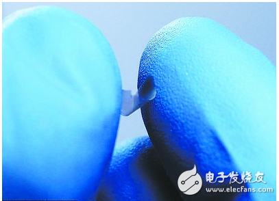
A team of scientists has recently developed a new type of material that is a thousand times thinner than paper, yet strong enough to not undergo structural changes even when bent. This microflake material is made of alumina and can be manually manipulated, although it is a nanoscale material.
This ultra-thin material can be used in the aerospace industry and even promote the rapid development of insect flying robot technology. Scientists have conducted many years of research to finally design the thinnest and lightest material. The material was designed by researchers at the University of Pennsylvania.
The person in charge of the project said that the nanoscale materials designed by scientists were very strong, but they are difficult to apply to the macro scale. Our ultimate goal is to create a stand-alone nano-scale thin layer of material, but its scale is large enough to be manually operated, which was previously impossible. This alumina thin layer material has a thickness between 25 and 100 nanometers and is stacked together at an atomic level.
Nanomaterials can be roughly classified into four types: nano powder, nano fiber, nano film, and nano block. Among them, nano-powder has the longest development time and the most mature technology, which is the basis for the production of other three types of products.
NanoceramicThe nano-ceramic materials developed by using nanotechnology are modified by using nano-powders, by adding or forming nano-sized particles, whiskers, wafer fibers, etc. to ceramics, so that grains, grain boundaries and between them The combination reaches the nano level, which greatly increases the strength, toughness and superplasticity of the material. It overcomes many of the deficiencies of engineering ceramics and has an important impact on the mechanical, electrical, thermal, and magneto-optical properties of materials, and opens up new fields for the replacement of engineering ceramics.
With the wide application of nanotechnology, nano-ceramics have emerged, hoping to overcome this
The brittleness of ceramic materials gives ceramics a metal-like flexibility and processability.
British materials scientist Cahn pointed out that nano-ceramics is a strategic way to solve the brittleness of ceramics. Nano high temperature resistant ceramic powder coating material is a material that forms a high temperature resistant ceramic coating by chemical reaction
Nano powderAlso known as ultrafine powder or ultrafine powder, generally refers to powder or granules with a particle size below 100 nm, which is a solid particulate material in an intermediate state between atoms, molecules and macroscopic objects. Can be used for: high density magnetic recording materials; absorbing stealth materials; magnetic fluid materials; radiation protection materials; single crystal silicon and precision optical device polishing materials; microchip thermal conductive substrate and wiring materials; microelectronic packaging materials; optoelectronic materials; Battery electrode material; solar cell material; high efficiency catalyst; high efficiency combustion improver; sensitive components; high toughness ceramic material (non-cracking ceramics, used in ceramic engines, etc.); human body repair materials; anti-cancer preparations.
NanofibersRefers to a linear material with a diameter of nanometer scale and a large length. Can be used for: micro-wires, micro-fibers (important components of future quantum computers and photonic computers) materials; new laser or light-emitting diode materials. The electrospinning method is a simple and easy method for preparing inorganic nanofibers.
NanofilmNanofilms are divided into granular membranes and dense membranes. The particle film is a film in which the nanoparticles are stuck together with a very small gap in between. A dense film refers to a film that is dense but has a grain size of nanometer. Can be used for: gas catalysis (such as automotive exhaust gas treatment) materials; filter materials; high-density magnetic recording materials; photosensitive materials; flat panel display materials; superconducting materials.
Nano-blockThe nano-block is a nano-grain material obtained by high-pressure molding or controlling the crystallization of a metal liquid. The main uses are: ultra-high strength materials; smart metal materials.
Application of several new nano -functional materials for the definition of nano-functional materialsNanomaterials refer to materials that have at least one dimension in the three-dimensional space in the nanometer scale range (1 to 100 nm) or are composed of them as basic units. It is precisely because the basic composition unit scale is small, nanomaterials have many effects that other common scale materials do not have, including volume effect, surface effect, dielectric confinement, quantum size, quantum tunnel, etc., the most notable of which is Volume effect and dielectric confinement. The volume effect means that the nanoparticles are small enough, and the catalytic properties, thermal resistance, internal pressure and light absorption of the nanomaterials have changed greatly. The nano absorbing coating made by using this property has light weight, thin thickness and absorbing wave. Frequency bandwidth and other advantages. The dielectric effect refers to the fact that when the nanomaterial is surrounded by a certain medium, the field strength of the nano surface and its vicinity increases due to the different refractive indices of different materials for light. This effect is widely used in photocatalysis in heterogeneous reactions. material. It is these unique effects that make nanomaterials have great application prospects in the fields of traditional materials, electronic equipment, medical equipment, machinery manufacturing, and military industry.
Application of nano-functional materials in the research of stealth materialsAt present, the research of deeper nanomaterials is mainly for the research of metal nanoparticles with broad application prospects in the fields of information storage, biomarkers and photographic technology, as well as cu nanomaterials which can be applied in the fields of catalysts, antibacterial agents and lubricating additives.
At present, the stealth materials that have been practically used mainly include electric loss type and magnetic loss type. The main principle is to convert electrical signals or magnetic signals into thermal energy or related energy forms to reduce the reflected signal intensity of the object to achieve stealth. The working principle of nano-stealth materials is mostly magnetic loss type. The micro-mechanism is that as the micro-scale of the material decreases, the number of surface atoms is relatively more and more, the activity of the material is enhanced, and the magnetic energy is converted into heat energy during the accelerated movement of the micro-particles, reducing the signal. reflection.
(1) Broadband: The so-called broadbandization means that the wavelength of the nano-stealth material can absorb the radar detection signal longer. With the continuous advancement of stealth technology, the military field began to use multi-frequency radar cooperative detection methods to combat, especially the development of meter- and millimeter-band radars put a great test on military aircraft stealth technology. At present, only stealth materials that can only absorb a few bands can no longer meet the actual requirements. It is important to study the preparation of nano-thin stealth materials with wide-band stealth.
(2) Thinning and thinning: By transforming the microstructure of existing nano stealth materials, improving the stealth performance while reducing the material density has become a key topic in the research of stealth materials. The specific method is to mix some specific ferromagnetic materials with nano materials to adjust the electromagnetic parameters to achieve the optimal effect.
Applied in the medical fieldCancer is a huge challenge for human health this year. The main reason why it is difficult to cure is that cancer cells are difficult to selectively eliminate with normal cells. Nanoparticle-encapsulated smart drugs can actively detect cancer cells and perform targeted elimination, especially magnetic nanometers. When the material is used as a drug carrier [3], the special magnetic field of the human body is used to make the drug aggregate and function in a specific region, which greatly reduces the risk of using the drug, and can also utilize the biodegradation characteristics of some nano materials to reduce the side effects of the drug, and utilize Nanocarriers inoculated with antigen or antibody were probed.
With the improvement of human ability to manipulate nanomaterials, nano-robots have developed rapidly. In order to build the scale of the basic materials used in nano-robots, nano-robots mainly include two types: one is to construct a mechanical or even a specific function of a robot on a molecular scale by manipulating atoms or molecules to achieve the purpose of phagocytizing diseased cells; The class is an organic combination of biological systems and mechanical systems represented by silicon wafer memories, which can cure diseases by affecting or changing the normal physiological metabolic processes of the human body.
Applied in the chemical industryDue to the extremely small size of nanomaterials and unique electrical, magnetic and optical properties, since the early 1980s, researchers have made many significant research achievements in the chemical industry by utilizing the volume effect, quantum size and surface effects of nano-functional materials.
Traditional catalysts have low catalytic efficiency and serious environmental pollution. The catalysts made by emerging nanomaterials have revolutionized the chemical industry by optimizing the reaction path and improving the catalytic efficiency. The basic principle is that the nano-materials have a relatively small number of surface particles, so the surface activity is extremely large, providing a large number of places for the polymerization and chain-breaking between molecules. Taking nanoparticles of Ni or Cu-Zn compounds as an example, these catalysts replace expensive platinum or button catalysts, and the nanoplatinum black catalyst can reduce the oxidation temperature of ethylene from 600 ° C to room temperature.
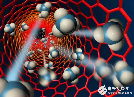
Carbon nanotubes can be used as reinforcing materials to form a variety of composite materials such as hydrogen storage materials. At present, it is possible to generate an arc between two graphite electrodes by 20V direct current, so that the anode is continuously evaporated at 4000K-10000K, causing arc spray to obtain nanoparticles, wherein 30% are carbon nanometers with a length of 3-10 nm and a diameter of 1-5 nm. Tube particles. Southwestern Nanotechnology Corporation has cooperated with Phillips of the mainland to realize the manufacture of multi-walled carbon nanotubes and single-walled carbon nanotubes by a fluidized bed reactor process.

Since the formal introduction of nanomaterials in the 1980s, basic theoretical research and practical product development have made significant progress. Taking 1997-2004 as an example, the investment in scientific research on nanomaterials worldwide has increased from 820 million to 3.2 billion. Nanomaterials have been widely used in chemical manufacturing, military spacecraft stealth, medicine and biology, such as volumetric effects, surface effects, and dielectric confinement. Nano-calcium carbonate, nano-silica, nano-zinc oxide, etc. All have formed a relatively large market size. China has achieved rapid development of the nano-industry through concentrated scientific research and increased investment by various leading enterprises. At present, based on low raw material prices and strong market demand, nano-calcium carbonate and nano-zinc oxide have formed industrial clusters or even complete industries. chain. But at the same time, it also faces the following problems:
First, the investment demand for nanomaterials research is large. The private-small SMEs have weak scientific research strength and the financial strength is generally not strong, and there is no need for national level support.
Second, the scientific research forces are scattered, the repeated labor is obvious, and there is no concentrated and orderly research echelon, and there is a lack of large-scale scientific research bases.
Third, the combination of production, education and research is insufficient. The research and application of nanomaterials to nanomaterials is weak, which limits the research and development of nano-functional materials, especially the high-purity and high-index nanomaterials.
PCB bus slot edge card sol: 1.27mm, 2.54mm, 3.175mm, 3.96mm, 90 degree, 180 degree dip plug-in board, SMT board, press type, welding type, ear, long pin series.
PCB bus slot edge card sol: 1.27mm, 2.54mm, 3.175mm, 3.96mm, 90 degree, 180 degree dip plug-in board, SMT board, press type, welding type, ear, long pin series
EDGE CARD SOLT
ShenZhen Antenk Electronics Co,Ltd , https://www.antenk.com