For designers who need to use large-scale FPGA devices on their PCBs, I/O pin assignments are one of the many challenges that must be faced. For a number of reasons, many designers have reported that it is increasingly difficult to determine I/O pin configurations or layout schemes for large FPGA devices and advanced BGA packages. But the combination of multiple intelligent I/O planning tools makes the pin assignment process easier.
Defining the I/O pinout of an FPGA device on a PCB is a daunting design challenge that can help the design complete quickly or it can cause design failure. In this process, both FPGA and PCB requirements must be balanced, and both designs must be completed in parallel. If pin layout optimization is only for PCB or FPGA, it may cause design problems on the other hand.
To understand the consequences of pin assignments, the PCB layout and FPGA physical device pins, as well as internal FPGA I/O points and associated resources, need to be visualized. Unfortunately, to date, there is no single tool or method that can satisfy all of these collaborative design needs at the same time.
However, different techniques and strategies can be combined to optimize the pin planning process and actively adopt new co-design tools such as Xilinx PinAhead technology to develop an effective pin assignment and layout method. Xilinx includes PinAhead in the ISE Software Design Suite 10.1.
Xilinx has developed a rule-driven approach. First define a set of initial pinouts based on PCB and FPGA design requirements, so that the pin layout design team, which is very close to the final version, can begin their design flow as early as possible. If adjustments are needed later in the design process due to PCB layout or internal FPGA performance issues, these issues are often localized in the early days of this design process, requiring only minor design modifications in the PCB or FPGA design.
Step 1: Evaluate design parametersSo where do you start? First, you should develop an I/O allocation strategy as early as possible. But without optimization tools or a complete netlist, it can be difficult to accomplish this task.
First, let's answer a few questions to determine PCB physical parameters and limitations:
* How many layers of PCB board, trace width, and via size?
* Does the PCB parameter limit the types of FPGA packages that can be used (such as BGA)?
* Is there a fixed interface location on the PCB that the FPGA must use? Other chips, connectors, or layout restrictions?
* Which high-speed interfaces require special attention?
Can you visualize your layout strategy to ensure the shortest interconnect?
You will find it helpful to draw a PCB layout. The PCB layout should include all major components as well as critical interfaces and buses to help determine the optimal FPGA pin assignment. Please note that the components are drawn on the actual mounting surface of the PCB. Label out interfaces that require special attention, such as high-speed buses and differential pairs (Figure 1).
Next, check the layout of the FPGA device to see where the physical resources on the chip are. List the different voltages and clocks used in the design and begin the isolation of the interfaces required for the design. Then determine if the design uses special I/O interface resources such as Gigabit Transceiver (GT), BUFR, IODELAY, and Digital Clock Manager. These resources may need to deploy the relevant I/O pins as close as possible to each other.
It is now necessary to determine the location of FPGA resources such as PowerPC, DSP48, and RAM16 used in the design. Place any relevant I/O connected to the I/O group as close as possible to the nearest resource. Then look at the ability to combine certain I/O signals into the interface, which is helpful for pin assignment. Finally, determine the configuration mode of the FPGA.
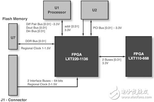
Figure 1 PCB connection diagram
Step 2: Define the pin layout requirementsOnce you understand the main FPGA interface and create a prototype of the physical layout, you can define the pin layout. Some designers prefer to use a data table containing all I/O signals to maintain a pin-to-pin correspondence. You can group them by voltage, clock, interface or bus. This method is really useful because it helps you group the signals into groups so that you can group them when you assign pins. At this stage, you will also find that in order to achieve optimal PCB layout, some critical interfaces must be placed on one side of the device or external physical pins.
After considering the FPGA and PCB requirements and determining the primary interface locations, the next step is to assign pins to the I/O banks based on all of these conditions. This is also the place to really start working. In the current design flow, a time-consuming task in pin assignments can involve many attempts and errors in resolving any performance and signal integrity issues. Traditionally, designers have done this task by hand, because EDA and chip vendors have not provided tools to help designers visualize FPGA and PCB pinouts.
But now Xilinx has provided the corresponding tools. The PlanAhead Lite included in the ISE FoundaTIon software tool version 10.1 is a simplified version of the PlanAhead design, analysis, and layout tools. Among them, PinAhead's tools for PCB and FPGA design make I/O pin configuration easier.
We are not going to go into all the details of the tool here, but just look at how to use it for I/O pin assignments. If you would like to learn more about PinAhead, including video presentations and tutorials, please visit.
Step 3: Pin assignment using PinAheadThe PinAhead environment provides a different set of views. Use these views to help complete the mapping and assignment of I/O port information to physical package pins or die I/O disks (Pad) (Figure 2).
2.54mm Pitch
2.54mm Pitch
HuiZhou Antenk Electronics Co., LTD , https://www.atkconn.com