Eamon Nash and Eberhard Brunner
The directional coupler is used to detect RF power and has a wide range of applications and can appear in multiple positions in the signal chain. This article discusses ADI's new device ADL5920, which integrates a broadband directional coupler and two RMS response detectors in a 5 mm × 5 mm surface mount package. Compared to traditional discrete directional couplers that have to make a difficult trade-off between size and bandwidth, this device has obvious advantages, especially at frequencies below 1 GHz.
Online RF power and return loss measurements are usually implemented using directional couplers and RF power detectors.
In Figure 1, the two-way coupler is used in radio or test and measurement applications to monitor the transmitted and reflected RF power. Sometimes it is also desirable to embed RF power monitoring in the circuit. A good example is to switch two or more signal sources to the transmission path (using RF switches or external cables).
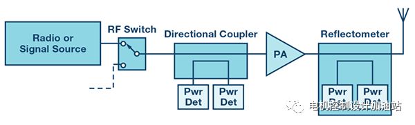
Figure 1. Measuring the forward and reflected power in the RF signal chain
The directional coupler has an important characteristic of directivity, that is, it can distinguish between incident and reflected RF power. When the incident RF signal passes through the forward path coupler (Figure 2) on the way to the load, it couples a small part of the RF power (usually a signal that is 10 dB to 20 dB lower than the incident signal) and enters the RF detector. When both forward power and reflected power are to be measured, another coupler must be used, the direction of which is opposite to the forward path coupler. The output voltage signals of the two detectors will be proportional to the forward and reverse RF power levels.

Figure 2. Typical RF power measurement system using directional coupler and RF detector
The basic problem of surface mount directional couplers is to make a trade-off between bandwidth and size. Although bidirectional directional couplers with a frequency coverage of one octave (that is, FMAX equals twice FMIN) usually use packages as small as 6 mm2, multi-octave surface mount directional couplers are much larger (Figure 3). Broadband connector-type directional couplers have multi-octave frequency coverage, but are significantly larger than surface mount devices.
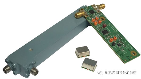
Figure 3. Connector type directional coupler, surface mount directional coupler, and ADL5920 integrated IC with directional bridge and dual RMS detector
Figure 3 also shows the ADL5920 evaluation board, which is a new RF power detection subsystem with a detection range of up to 60 dB. It is packaged in a 5 mm × 5 mm MLF (ADL5920 IC is located between the RF connectors). The functional block diagram of ADL5920 is shown as in Fig. 4.
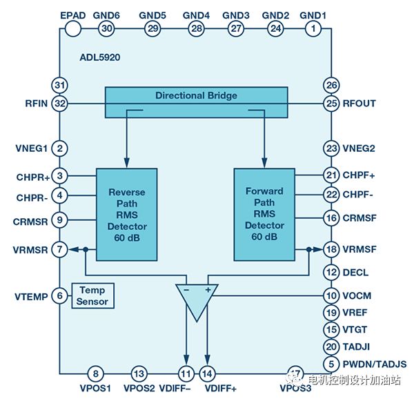
Figure 4. Block diagram of ADL5920
The ADL5920 does not use a directional coupler to detect forward and reflected signals, but uses a patented directional bridge technology to achieve broadband and compact on-chip signal coupling. To understand the working principle of the directional bridge, we need to review the Wheatstone bridge first.
Wheatstone Bridge
The concept of the directional bridge is based on the Wheatstone bridge (Figure 5), that is, the differential voltage generated at equilibrium is zero. In the Wheatstone bridge, one resistance in one of the two branches is variable (R2), while the other two resistances (R1 and R3) are fixed. There are a total of four resistors-R1, R2, R3 and Rx, where Rx is the unknown resistance. If R1 = R3, then when R2 is equal to Rx, VOUT = 0 V. When the variable resistor has an appropriate value to make the voltage divider ratios on the left and right sides of the bridge equal, so that a 0 V differential signal is generated at the differential detection node that generates VOUT, the bridge is considered to be in a balanced state.
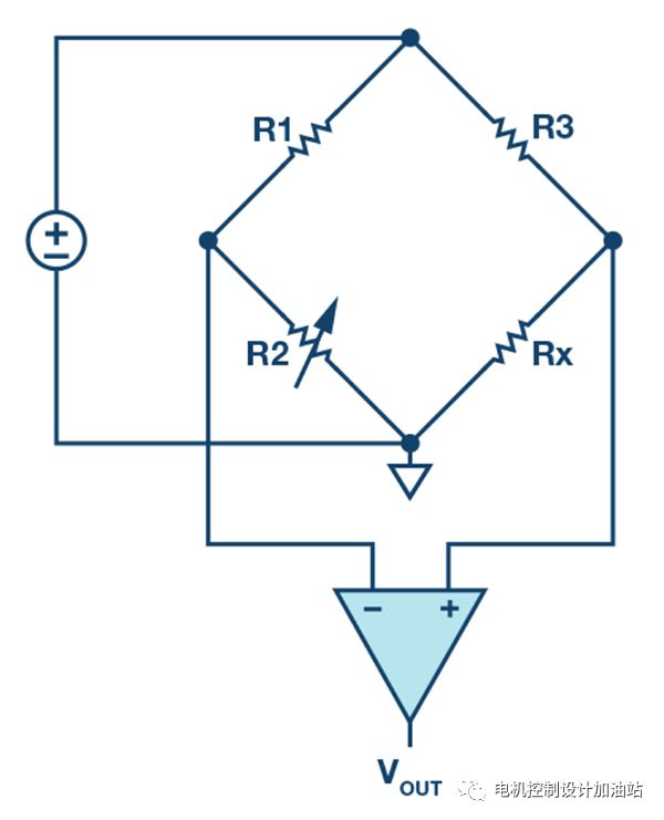
Figure 5. Wheatstone bridge
One-way bridge
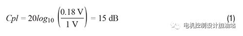
Figure 6 is a schematic diagram of a unidirectional bridge, which explains the basic operation of this device very well. The first thing to note is that the directional bridge needs to be designed for a specific Zo and minimize the insertion loss. If RS = RL = R = 50, the detection resistance of the bridge is 5, so the insertion loss (port impedance, and calculating RIN will get 50.8 port impedance (|Γ| = 0.008; RL = –42 dB; VSWR = 1.016) If the signal shown in RFIP is applied, since RIN is about 50, the voltage at RFIP is about half of the power supply voltage. Assuming that the voltage at RFIP is equal to 1 V, the voltage at RFOP is about 0.902 V.
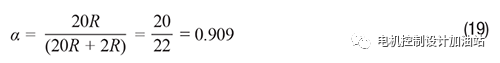
This voltage is further attenuated by 10/11 = 0.909, making the negative input of the differential amplifier 0.82V, and the resulting differential voltage is (1 – 0.82) = 0.18 V. The effective forward coupling factor (Cpl) of the bridge is
In terms of the bridge, balance means that when the signal is applied in the reverse direction (RFOP to RFIP), the VFWD detector (or Cpl port) will see zero differential voltage under ideal conditions, and when the signal is applied in the forward direction (RFIP to RFIP). RFOP), what you see will be the largest signal. In order to obtain maximum directivity in this structure, precision resistors are the most important, so it is beneficial to integrate them.
In a unidirectional bridge, in order to determine the isolation required to calculate the return loss, the device needs to be flipped, and then the input signal is applied to the RFOP. In this case, the bridge is balanced and the positive and negative inputs of the differential amplifier are equal, because the same voltage divider ratio 0.909 = (10R/(10R + R) = (R/(R+0.1R)) results in a differential voltage (V+ minus V-) = 0 V.
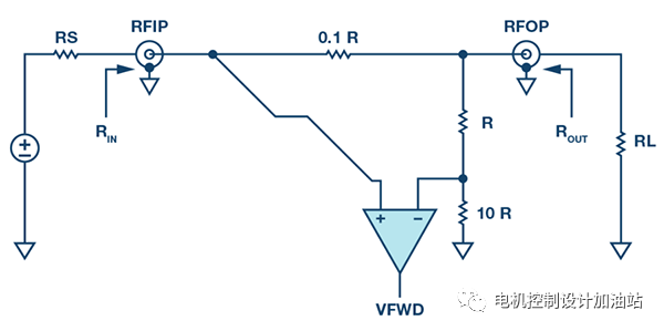
Figure 6. Simplified unidirectional bridge circuit diagram
Two-way bridge
Figure 7 is a simplified diagram of a two-way bridge, similar to the one used in ADL5920. For a 50 environment, the unit resistance R is equal to 50. Therefore, the detection resistance value of the bridge is 5, and the resistance value of the two shunt networks is about 1.1 k.
This is a symmetrical network, so when RS and RL are also equal to 50, the input and output resistances RIN and ROUT are the same and close to 50.
When the source impedance and load impedance are both 50, the ohmic analysis of the internal network tells us that compared to VREV, VFWD will be quite large. In practical applications, this corresponds to the maximum power transmission from the signal source to the load. This results in very small reflected power, which in turn results in very small VREV.
Next, we consider what happens if RL is infinite (open circuit) or zero (load shorted). In both cases, if we repeat the Ohm analysis, we will find that VFWD and VREV are roughly equal. This reflects that the forward and reflected power are equal in an actual system in the case of an open circuit or a load short circuit. These situations will be analyzed in more detail below.
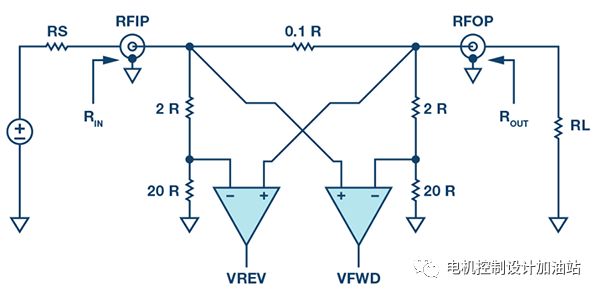
Figure 7. Simplified two-way bridge circuit diagram
VSWR and reflection coefficient
A comprehensive analysis of errors in network analysis is too complicated and beyond the scope of this article, but we want to outline some basic concepts here. The application note "Directivity and VSWR Measurement" written by Marki Microwave is an excellent article for reference 1.
Traveling wave is an important concept to describe the voltage and current on the transmission line because it is a function of position and time. The general solution of the voltage and current on the transmission line includes a forward traveling wave and a reverse traveling wave, which are functions of distance x2.
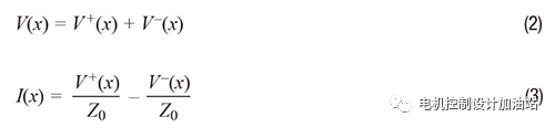
In Equation 2 and Equation 3, V+(x) represents the voltage wave traveling toward the load, and V–(x) represents the voltage wave reflected from the load due to mismatch, and Z0 is the characteristic impedance of the transmission line. In a lossless transmission line, Z0 is defined by the following classic equation:
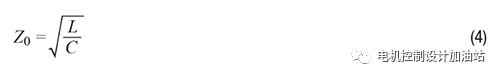
The most common Z0 for transmission lines is 50. If such a line is terminated with a characteristic impedance, it is an infinite line from the point of view of the 50 signal source, because any voltage wave traveling along the line will not be generated and can be detected at the signal source or anywhere else on the line Reflection. However, if the load is not 50, then a standing wave will be generated along the line, which can be detected, which is defined by the voltage standing wave ratio (VSWR).
More generally, the reflection coefficient is defined as:
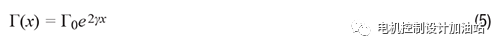
Where Γ0 is the load reflection coefficient and is the propagation constant of the transmission line.
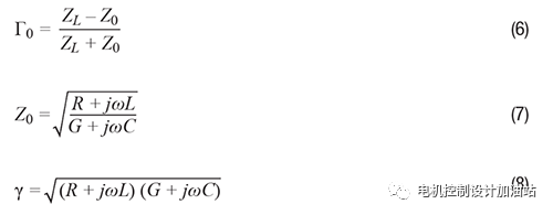
R, L, G, and C are the resistance, inductance, conductance and capacitance per unit length of the transmission line, respectively.
Return loss (RL) is the negative value of the reflection coefficient (Γ), measured in dB. This is important because reflection coefficient and return loss are often confused and used interchangeably.
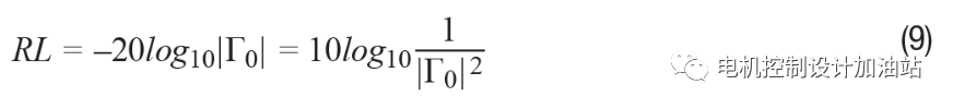
In addition to the above-mentioned load mismatch, return loss has a very important definition, which is defined according to the incident power and reflected power at the impedance discontinuity, as shown below:
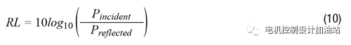
It is widely used in antenna design. The relationship between VSWR, RL and Γ0 is as follows:
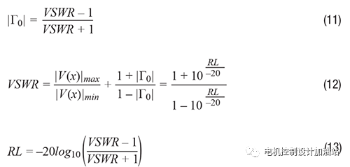
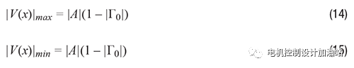
Equations 14 and 15 represent the maximum and minimum values ​​of the standing wave voltage, respectively. VSWR is defined as the ratio of the maximum voltage to the minimum voltage on the wave. The peak voltage and minimum voltage on the line are:
For example, in a 50 transmission line, if the peak amplitude of the forward traveling voltage signal A = 1, and the line matches an ideal load, then |Γ0| = 0, there is no standing wave (VSWR = 1.00), and the peak voltage on the line is A=1. However, if RLOAD is 100 or 25, then |Γ0| = 0.333, RL = 9.542 dB, VSWR = 2.00, |V(x)|max = 1.333, |V(x)|min = 0.666.
Figure 8 is a copy of Figure 7, but the signal shown uses the default forward configuration and indicates the traveling power wave, with the reference plane at the load. At low frequencies, the wavelength is longer relative to the physical structure, the voltage and current are in phase, and the circuit can be analyzed according to Ohm's law.
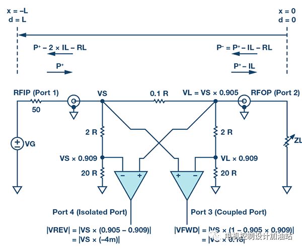
Figure 8. Simplified two-way bridge with signal
The ports are defined as follows: the input port (port 1) is RFIP, the output port (port 2) is RFOP, the coupling port (port 3) is VFWD, and the isolation port (port 4) is VREV. Because the structure is symmetrical, when the signal is reflected at ZL or applied to RFOP, the port is reversed.
When the load is matched and the generator voltage is connected to port 1 (RF IP), ZS = ZL = Z0 = R = 50,
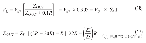
VL/VS+ is the insertion loss LI or IL, in dB.

The attenuation factor of the two parallel branches on either side of the 0.1×R main line resistance is:
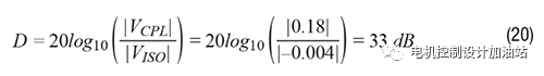
The |VREV| and |VFWD| formulas in Figure 8 show the voltage value when the signal is applied in the forward direction. These formulas point out the basic directivity limitation of the simplified schematic because the rejection performance (33 dB) of the isolated port is not ideal.
As can be seen from Figure 8, the directivity of the bidirectional bridge in the linear domain is determined by the following formula:
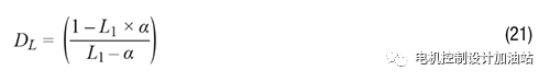
This means that in order to improve the directivity, it needs to be equal to the insertion loss L1.
In silicon wafers, the peak directivity is usually better than indicated by the diagram (Figure 9).
If ZL is not equal to ZO (under normal conditions), the coupling and isolation port voltage (complex) will be:
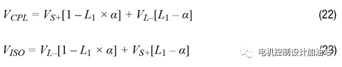
Among them, VS+ is the forward voltage at port 1 (node ​​VS), and VL- is the reflected voltage of the load at port 2 (node ​​VL). Is the unknown phase of the reflected signal,
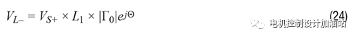
Use (24) to replace VL- in (22) and (23), and use (21) to simplify the result. In addition

The output voltage is very complicated.
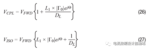
It can be seen from (26) and (27) that when DL>>1,
In the ADL5920, the voltages VREV and VFWD are respectively mapped to the voltages VRMSR and VRMSF through two linear dB RMS detectors in the 60 dB range, respectively (VISO/VSLP) and (VCPL/VSLP). So the device’s differential output VDIFF (in dB) means
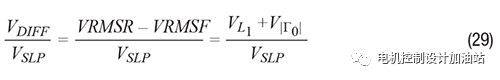
The slope VSLP of the detector is about 60 mV/dB.
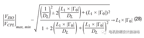
Using the voltage to dB mapping of (29) in (28),
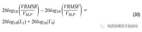
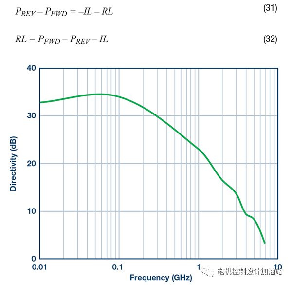
Figure 9. The relationship between ADL5920 directivity and frequency. The input level is 20 dBm
Figure 10 shows the response of the forward power detection RMS detector when the ADL5920 is driven forward. Each curve corresponds to the relationship between output voltage and frequency at a specific applied power level. The curve stops at 10 MHz, and operation at frequencies as low as 9 kHz has been verified. In Figure 11, the same data is expressed as the relationship between output voltage and input power, and each trace represents a different frequency.
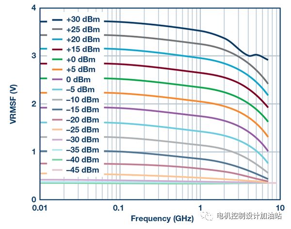
Figure 10. Typical output voltage versus frequency of a forward path detector at various input power levels

Figure 11. Typical output voltage vs. input power of the forward path detector at multiple frequencies
When the RFOUT pin of ADL5920 is terminated with a 50 Ω resistor, there should be no reflected signal. Therefore, the reverse path detector should not record any detected reverse power. However, since the directionality of the circuit is not ideal and will roll off with frequency changes, some signals will be detected in the reverse path. Figure 12 shows the voltages measured by the forward and reverse path detectors when scanning RFIN and RFOUT is terminated with a 50 resistor at a frequency of 500 MHz. The vertical pressure difference between these traces is directly related to the directionality of the bridge.
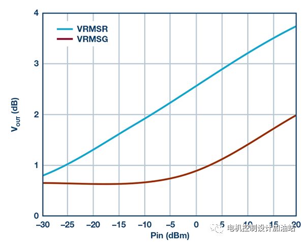
Figure 12. The relationship between VRMSF and VRMSR output voltage and input power, 500 MHz, the bridge is driven from RFIN, and RFOUT is terminated with 50 Ω
Figure 13 shows the effect of changing the load on the forward power measurement. The specified power level is applied to the RFIN input, and the load return loss on RFOUT changes from 0 dB to 20 dB. As expected, when the return loss is in the range of 10 dB to 20 dB, the power measurement accuracy is very good. But as the return loss drops below 10 dB, the power measurement error begins to increase. It is worth noting that when the return loss is 0 dB, the error is still within 1 dB.
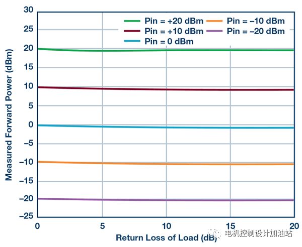
Figure 13. The relationship between the measured forward power and the applied power and the return loss of the load, measured at 1 GHz
In Figure 14, ADL5920 is used to measure the return loss of the load, and the frequency is also 1 GHz. Apply a known return loss to the RFOUT port. Measure VRMSF and VRMSR, and reverse the return loss.
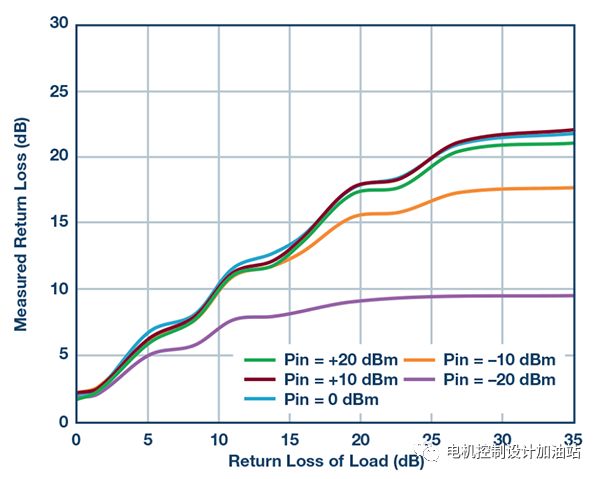
Figure 14. The relationship between the measured return loss and the applied return loss and RF power, measured at 1 GHz
There are a few things to note about this diagram. First of all, it can be seen that as the return loss improves, the ability of the ADL5920 to measure return loss decreases. This is because the device has directivity. Secondly, please pay attention to how the measurement accuracy decreases as the driving power decreases. This is due to the limited detection range and sensitivity of the ADL5920 onboard RMS detector. The third point is related to the obvious ripples in the trace. This is because each measurement is made in a single return loss phase. If the measurement is repeated in all return loss stages, a series of curves will be produced, the vertical width of which will be approximately equal to the vertical width of the ripple.
application
With the ability to measure RF power and return loss online, the ADL5920 can be used in a variety of applications. Its small size means it can be placed in many circuits without much impact on space. Typical applications include online RF power monitoring (RF power levels can be as high as 30 dBm, where insertion loss is not important). The return loss measurement function is usually used in applications that need to monitor RF loads. This can be a simple circuit to check if the antenna is damaged or broken (ie catastrophic failure). However, the ADL5920 can also measure scalar return loss in materials analysis applications. This is most suitable for applications with frequencies below about 2.5 GHz, where the directivity (and thus the measurement accuracy) is greater than 15 dB.
The ADL5920 evaluation board has two dimensions, as shown in Figure 15. Shown on the left is a traditional evaluation board, the detector output voltage can be provided through clip-on leads and SMA connectors. The evaluation board also includes a calibration path that can be used to calibrate the insertion loss of the FR4 board.
The evaluation board shown on the right is more integrated and includes a 4-channel 12-bit ADC (AD7091R-4). This evaluation board can be connected to ADI's SDP-S USB interface board, and it contains PC software that can calculate RF power and return loss, and perform basic power calibration routines.
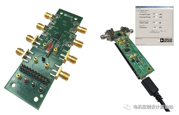
Figure 15. ADL5920 evaluation board selection
Gan 150W,Usb Pd Charger,Charger Gan,Gan Adapter
ShenZhen Yinghuiyuan Electronics Co.,Ltd , https://www.yhypoweradapter.com