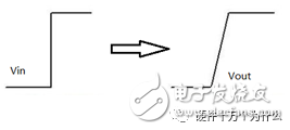
To do a 1pps driver circuit, the rising edge is required to be ≤5ns. After the signal output from the FPGA is followed by the enhanced driver with the op amp, it is found that the rising edge does not meet the requirements. why? Because it does not take into account an important indicator, the slew rate. The slew rate is the average of the time-varying rate of the output voltage of the closed-loop amplifier when the input is a step signal. That is, input an ideal step signal, the output will be a signal with a slope, and the rate of climb of this signal is the slew rate.
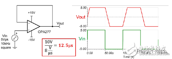
Take a look at the slew rate of this op amp:
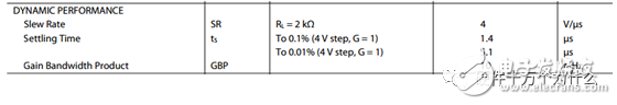
It can't meet the requirements at all. 5ns can only climb 20mV, so the rising edge can't meet the design requirements. How to do it? A pulse boost circuit has been added to the late fly line.
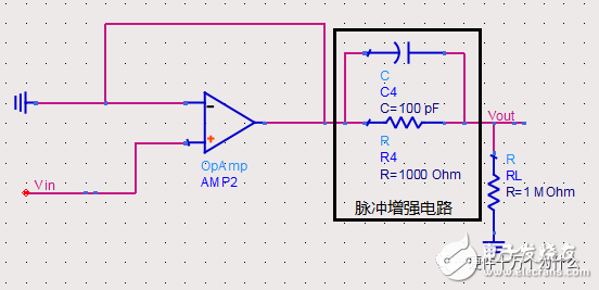
The pulse enhancement circuits C4 and R4, which correspond to a differentiating circuit C4 and RL (when C x RL is much smaller than the slew rate time) plus a DC resistor R4, make the signal edges on the load RL steeper. Analyze:
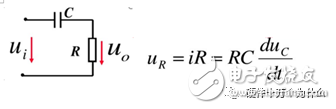
a. Capacitor C4 and RL form a voltage dividing circuit. According to the calculation formula of the following figure, the rate of change of voltage on C4 is equal to the voltage value on RL.
b. Then assume that the capacitance voltage change rate is almost unchanged in the range of 0-Ï„, then the voltage above the load RL is almost constant. Once the capacitor starts to charge (voltage changes), the voltage of the load RL rises to the top. . Recorded as waveform 1, as shown below.
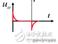
c. Then start to fall after the capacitor is charged. In order to solve the problem that there is no voltage without change rate, add a DC resistor R4 to maintain the waveform. It is a through waveform, which is the original waveform, which is recorded as waveform 2.
d. After the two waveforms are combined, the rising edge of waveform 2 is greatly enhanced due to waveform 1, so that the rising edge of the synthesized waveform is improved.
7. Seven of the ten holes of the operational amplifier - feedback resistor of the current feedback type operational amplifier
In order to expand the external drive capability, a follower circuit is generally added at the last stage, and the current feedback op amp-CFA is selected to increase the output bandwidth of the op amp. It’s so simple, but unfortunately you can’t adjust it. Or look at the picture first. It’s so simple, but unfortunately you can’t adjust it. Or look at the picture first.
What power rail, common mode input range, gain product bandwidth, load capacity, slew rate. . . I have all considered it, or is it wrong?
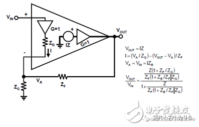
Because CFA and VFA (voltage feedback op amp) are not the same , the op amps that are used in reading, basically the teachers use VFA to give examples and explanations. The figure below is a model of the CFA op amp:
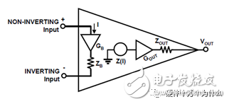
It differs from VFA in that the input is no longer both imaginary, the inverting input resistance ZB is a very small value, but it must not be considered zero; its open loop gain Gout is no longer very large, but It is approximately equal to 1; its transimpedance Z can be considered to be infinite.
Therefore, the circuit model of the CFA follower circuit is as follows:
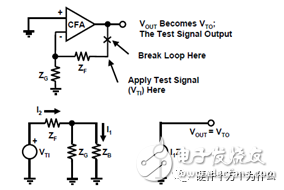
Solving Aβ is equal to:
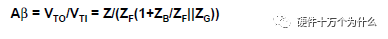
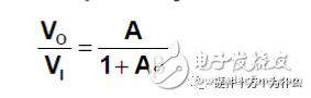
Its closed loop gain is:
When there is no feedback resistance ZF, A is approximately equal to 1, ZF approaches 0, Aβ approaches infinity, and the gain approaches 0, which is completely different from the desired follower circuit, which is often referred to as “CFA not on the Internetâ€. There is no signal when adding a feedback resistor." (I didn't find this sentence, I forgot where I saw it. I can only see the introduction of feedback resistors in the CFA manual.)
Therefore, to add a feedback resistor, the circuit will work properly.
PS: The above derivation calculation is tricky and can only be derived from Aβ calculation, because the calculation premise of CFA is that the inverting input resistance ZB is a very small value; its transimpedance Z can be considered as infinite, so the limit is Find a single variable, if you want to find the limit according to the final expression, a function, three variables (ZF approaches 0, ZB approaches 0, Z approaches infinity), can't play, as shown below.
8, eight of the eight pits of the operational amplifier - the failed AD620
In the era when I was in college, the instrumentation amplifier was definitely a high-X word. In the era when the three-operational amplifier was also used as a differential op amp, the instrumentation was synonymous with ultra-high common-mode rejection ratio and high temperature stability. In the opposite phase, the two voltage differences are reduced, and the result is obtained. This is definitely a good thing to collect EEG signals (Electroencephalogram (EEG) is a method of recording brain activity using electrophysiological indicators).
Because the EEG signal amplitude is small, plus the preamplifier, but also about 1V, so there is no problem with trial and error. Later, to do an industrial field signal detection, it is not normal. Or look at the picture first:
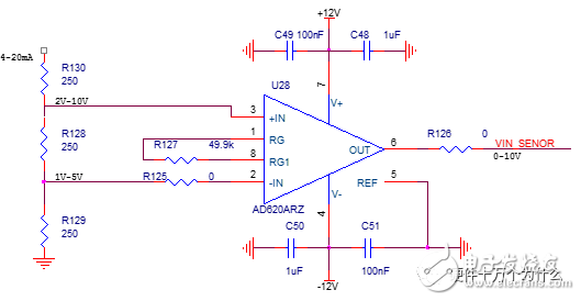
Collect 4-20mA current, get 1V-5V voltage difference, zoom in 2 times and enter the post-stage ADC. In order to prevent the power consumption of the resistor from being too high, the three resistors R128, R129 and R130 adopt the parallel value, and finally get the value of 250Ω.
Analysis, the positive phase input terminal 2V-10V, in line with the device input range (VCC-1.4V), inverting input terminal 1V-5V, I added negative power, it is more consistent; then see the magnification factor 2 times, Vmax = 10V, also meets the device output range (VCC-1.4V); power supply, amplification, decoupling, etc. are no problem. This is a schematic that appears to have no errors, but in reality it will make an error at high input voltage values.
Look at the internal principle of the instrument, you will understand (here choose a hand on the information, not the internal principle of the AD620, in fact, the principle of the instrument is similar)
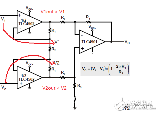
The positive phase input voltage and the inverting input voltage are reflected in the R2 inside the instrument, and the actual output voltage is reflected by V1out and V2out. In other words, the final added voltage value is divided into two parts, one by V1out provides, it will be higher than V1, and the other is provided by V2out, which will be lower than V2.
Looking at the schematic diagram, at 20 mA, Vin+ reaches 10V, Vin- is 5V, and is amplified by 2 times. In the instrument, it is necessary to enlarge Vin+ to 12.5V. This has exceeded the supply voltage of the instrument, so it is absolutely impossible to work properly.
9. Nine of the ten holes of the op amp - the sampling time of the ADC is dragged down by the op amp
The ADC collects signals, and when the signal is stable, it is very accurate; when the signal changes, the data is unstable. Of course, the ADC has sampling time, and the software engineer knows that he took 10 times and only took it 5 times, but the data is still unstable. Let the hardware look at the circuit. The hardware engineer said that the circuit is of course no problem. It is all deducted from others. How can I have problems with me?
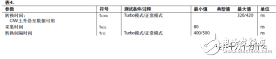
First look at the ADC's indicators Tcycmin = 500ns and Tacqmin = 80ns, this is a SAR ADC, the speed can be Mbps, fairly fast. Therefore, it is sampled 10 times in a row, and the time taken is only about 10 μs.
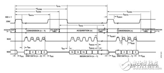
The op amp from the signal input to the output is not a process without delay, but a process with delay and oscillation. At the same time, the time of this process will increase due to the PCB design of the subsequent circuit. As shown below:
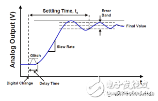
Look at the op amp's specifications. When 4V, it reaches 0.01%, the time is 5.1μs, and the fluctuation error is 0.4mV. In the 4V range, the 1LSB of a 16-bit ADC is 0.06mV. The error can eat 6, 7 code words. If the distributed capacitance and the trace resistance are added, this time will increase further, making the post-stage stabilization time increase, resulting in a larger error.

Later, the software engineer lowered the sampling rate, increased the acquisition time, and solved the problem.
10, the 10th hole of the op amp - the forgotten power consumption
I have done a board and the power consumption is very strict. Therefore, after the design is completed, I draw a power tree and calculate the power consumption of each device. There is no super, then the board is commissioned, debugged, powered on, and the power consumption exceeds the standard. .
After a check, it was found that there was a problem in the calculation of the op amp power consumption. Five of the op amp circuits used in the figure below.
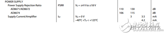
Because it is a DC drive, in the calculation, only the static power consumption of the op amp itself is considered, PD=15V x 4.2mA =63mW. According to the maximum static power consumption, the power consumption margin is more than enough.
In fact, an important power consumption point is neglected: the voltage difference between the op amp supply voltage of 15V and the output voltage (1V-4.5V) is all consumed in the op amp. According to the maximum differential voltage, one circuit consumes 140mW. This kind of dissipated power has never been considered before, so all of them are selectively ignored. When the demand for power consumption is tight, the problem is exposed.
Â
Later, when the version was changed, the low voltage was selected to supply power to the op amp, which reduced the dissipated power consumption and met the requirements of the index.
Membrane switch is an operating system that integrates key functions, indicating elements and instrument panels. It consists of four parts: panel, upper circuit, isolation layer and lower circuit.
When the membrane switch is pressed, the contacts of the upper circuit are deformed downward, and are in contact with the pole plate of the lower circuit.
After the finger is released, the contacts of the upper circuit bounce back, the circuit is disconnected, and the circuit triggers a signal. The membrane switch has strict structure, beautiful appearance and good sealing performance. It has the characteristics of moisture resistance and long service life.
Widely used in electronic communication, electronic measuring instruments, industrial control, medical equipment, automobile industry, smart toys, household appliances and other fields.
Can provide customers with professional product design. We HAVE accumulated MANY years of experience in Japanese customers, the company has stable quality management experience in mass production orders and can meet the customer's delivery time requirements and quality requirements on time. Now our products are widely used in communications, medical, electronics, digital, watches, automobiles and other high-end fields. With the ISO9001 factory certification, we have gradually become the industry leader with good management, leading technology, excellent quality, timely delivery and thoughtful service.
Membrane Switches, Poly Membrane Switches, Home Appliance Membrane Switch, Membrane Switch with Leds China Diy Membrane Switch
KEDA MEMBRANE TECHNOLOGY CO., LTD , https://www.kedamembrane.com